Location:Home Page > Archive Archive
How to make anti-interference PCB design?
2023-03-31【Archive】
The main task of anti-interference is to ensure that a system or device does not malfunction and does not lose performance due to external electromagnetic interference, and also does not create excessive noise interference to outside world so as not to affect normal operation of other systems or devices. Therefore, improving noise immunity of system is also an important part of system design.
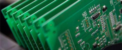
Summary of anti-jamming circuit design principles
1. Power Cord Design
(1) Select a suitable power supply;
(2) Make power cord as wide as possible;
(3) Make sure that direction of power line, bottom line and data transfer direction are same;
(4) Use anti-interference components;
(5) Add a decoupling capacitor (10~100uF) to power input.
2. Ground wire design
(1) separate analog and digital grounds;
(2) Try using single point grounding;
(3) Make ground wire as wide as possible;
(4) Connect sensitive circuits to a stable ground;
(5) Perform baffle design on PCB to separate high frequency noise circuit from low frequency noise circuit;
(6) Minimize area of the ground loop (the path formed by all devices that are grounded and returned to ground is called "ground loop").
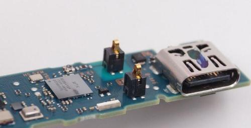
3. Component Configuration
(1) Do not use too long parallel signal lines;
(2) Make sure PCB clock, crystal oscillator and processor clock input are as close as possible to each other, while keeping away from other low frequency devices;
(3) Components should be placed around main device to minimize lead lengths;
(4) PCB separation diagram;
(5) Consider position and direction of PCB in chassis;
(6) Shorten wires between high frequency components.
4. Decoupling capacitor configuration
(1) Add charge/discharge capacitor (10uF) for every 10 ICs;
(2) Lead capacitors are used for low frequencies and chip capacitors for high frequencies;
(3) Each integrated chip must have a 0.1uF ceramic capacitor;
(4) The ability to withstand noise is weak, and device with large power changes when turning off must be equipped with high-frequency decoupling capacitors;
(5) Do not use common vias between capacitors;
(6) The lead wire of the decoupling capacitor must not be too long.
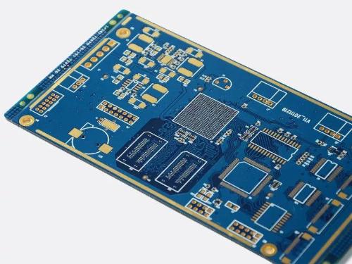
5. Noise and EMI Reduction Principles
(1) Try using a 45° polyline instead of a 90° polyline (to minimize external radiation and high frequency interference);
(2) Use series resistors to reduce frequency of edge jumps in circuit;
(3) Crystal oscillator case must be grounded;
(4) Do not pause idle channels;
(5) When clock is perpendicular to I/O line, there is little interference;
(6) Try to keep electromotive force tending to zero around clock;
(7) The I/O drive circuit should be as close to edge of PCB as possible;
(8) Don't loop for any signal;
(9) For high frequency boards, distributed capacitance of capacitor cannot be ignored and distributed capacitance of inductor cannot be ignored;
(10) Normally, power line and AC line should be on a different board from signal line.
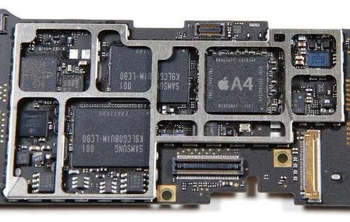
6. Other Design Principles
(1) Unused CMOS pins must be grounded or powered through resistors;
(2) Use an RC circuit to absorb discharge current of original components such as relays;
(3) Adding about 10 kΩ pull-up resistors to bus is useful for noise suppression;
(4) Using full decoding provides better protection against interference;
(5) Components do not use pins to connect to power supply via 10k resistors;
(6) The bus should be as short as possible and remain as long as possible;
(7) Wiring between two layers should be as vertical as possible;
(8) Heating components avoid sensitive components;
(9) The front side is wired horizontally and back side is wired vertically. If space permits, thicker better (ground and power lines only);
(10) For construction line to be good, it should be laid as far as possible in front, and reverse side should be used as construction line;
(11) Keep a sufficient distance, such as filter input and output, optocoupler input and output, AC power line and weak signal line, etc.;
(12) Long line plus low pass filter. Traces should be cut as short as possible, and long traces should be inserted into a C, RC, or LC low pass filter at a reasonable location;
(13) In addition to ground wire, do not use thick wires if thin wires can be used.
7, wire width and current
(1) Overall width must not be less than 0.2 mm (8 mils);
(2) On printed circuit boards with high density and precision, line spacing and line width are generally 0.3mm (12 mils);
(3) When copper foil thickness is about 50um, wire width is 1~1.5mm (60mil) = 2A;
(4) The public area is typically 80 mils, and more consideration should be given to microprocessor applications.
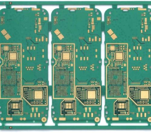
8. Power cord
The power cord should be as short as possible and run in a straight line, preferably in a tree shape rather than a loop.
9. Layout
First, pay attention to size of PCB. When PCB size is too large, printed lines will be long, impedance will increase, noise reduction capability will decrease, and cost will also increase; if it is too small, heat dissipation will be poor and adjacent lines will be easily broken.
After determining size of PCB, determine position of special components. Finally, according to functional block of circuit, all circuit components are decomposed.
The following principles should be observed when locating special components:
(1) Shorten coupling between high-frequency components as much as possible, try to reduce their propagation parameters and mutual electromagnetic interference. Components susceptible to interference should not be placed too close to each other, and input and output components should be placed as far apart as possible.
(2) There may be a large potential difference between some components or wires, and distance between them must be increased to avoid accidental short circuit caused by discharge. High voltage components should be placed out of reach of hands during debugging.
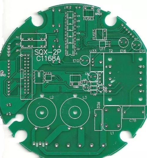
(3) Components weighing more than 15g must be stapled and then soldered. Those components that are large, heavy, and generate a lot of heat should not be installed on PCB, but should be installed on bottom plate of chassis of whole machine, and problem of heat dissipation should be considered. The thermal components must be kept away from heating components.
(4) When placing adjustable components such as potentiometers, adjustable inductors, variable capacitors and microswitches, structural requirements of entire machine should be taken into account. If it is adjustable inside machine, it should be placed on PCB in a convenient place for adjustment, if it is adjustable outside machine, then its position should be adapted to position of adjustment knob on chassis panel.
(5) The position occupied by plate positioning hole and fixing bracket must be reserved.
When placing all circuit components according to functional nodes of circuit, following principles must be observed:
(1) Arrange each functional unit of circuit according to flow of circuit, make layout convenient for signal to pass through, and keep signal in same direction as much as possible.
(2) Take main component of each function diagram as center and create a layout around it. Components should be placed flat, neat and compact on PCB Minimize and shorten pins and connections between components.
(3) For circuits operating at high frequencies, distribution parameters between components should be taken into account. As a general rule, circuit should place components in parallel as much as possible. Thus, it is not only beautiful, but also easy to assemble and weld, as well as mass-produced.
(4) Components located at edge of PCB are typically at least 2mm from edge of PCB. The best shape for a PCB is a rectangle. Aspect ratio 3:2 in 4:3. If PCB size exceeds 200x150mm, mechanical strength of PCB must be taken into account.
10. Wiring
The connection principles are as follows:
(1) The wires used for input and output terminals should not be maximally parallel to each other. It's best to add a ground wire between lines to avoid feedback.
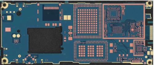
(2) The minimum width of printed photoconductive wire is mainly determined by adhesive strength between wire and insulating substrate and amount of current flowing through them. When thickness of copper foil is 0.05mm and width is 1~15mm, temperature will not be higher than 3°C when passing a current of 2A, so wire thickness of 1.5mm can meet requirements.
For integrated circuits, especially digital circuits, wire thickness of 0.02~0.3mm is generally selected. Of course, if allowed, use as wide wires as possible, especially power wires and ground wires. The minimum distance between conductors is mainly determined by worst case insulation resistance between lines and breakdown voltage. For integrated circuits, especially digital circuits, if manufacturing process allows, pitch can be as low as 5–8 mm.
(3) The corners of printed wires are usually arcuate, and right angles or included angles affect electrical performance in high frequency circuits. Also, try to avoid using a large area of copper foil, otherwise copper foil will easily stretch and fall off if heated for a long time. When a large area of copper foil needs to be used, it is best to use a mesh to eliminate volatile gases released by adhesive between copper foil and substrate when heated.
11. Gasket
The center hole of pad should be slightly larger than wire diameter of device. If pad is too large, a virtual solder seam can be easily formed. The outer diameter D of block, as a rule, is not less than (d + 1.2) mm, where d is diameter of outlet. For high-density digital circuits, minimum pad diameter can be (d+1.0) mm.
12, anti-interference measures for printed circuit boards and circuits
The design of anti-interference circuit boards is closely related to specific circuits. Here we will explain only some common anti-interference measures in PCB design.
13. Power Cord Design
Depending on amount of circuit board current, try increasing power line width to reduce loop resistance. At same time, direction of power line and ground line should match direction of data transmission, which helps improve the ability to resist noise.
14. Ground wire design
Ground wire design principles:
(1) Digital ground is separate from analog ground. If PCB has both logic circuits and line circuits, they should be separated as much as possible. The ground of low frequency circuit should be connected in parallel with one point as far as possible. When actual wiring is difficult, it can be partially connected in series and then connected in parallel. The high-frequency circuit should have a multi-point series ground, ground wire should be short and short, and a large-area grid-shaped ground foil should be used as much as possible around high-frequency components.
(2) The ground wire should be as thick as possible. If ground wire is made of thin wire, ground potential will change as current changes, which will reduce anti-noise performance. Therefore, ground wire must be thicker so that it can carry three times current allowed on PCB. If possible, ground wire should be higher than 2~3mm.
(3) The ground wire forms a closed loop. For printed circuit boards consisting only of digital circuits, ground circuit is usually arranged in a group loop to improve noise immunity.
15. Decoupling Capacitor Configuration
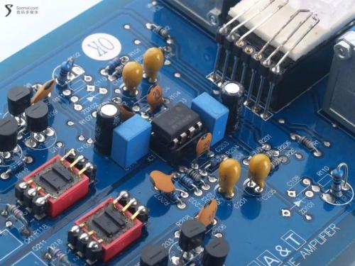
One common practice in PCB design is to install appropriate decoupling capacitors in various key parts of PCB.
General principle for configuration of a decoupling capacitor:
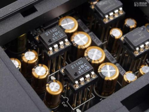
(1) Connect a 10-100uF electrolytic capacitor to input terminal of power supply. If possible, it is better to connect more than 100uF.
(2) In principle, each integrated circuit chip should be equipped with a 0.01pF ceramic capacitor. If there is not enough space on PCB, a 1-10pF capacitor can be installed for every 4-8 chips.
(3) For devices with weak anti-noise capability and large power-off changes, such as RAM and ROM storage devices, a decoupling capacitor should be directly connected between power line and ground line of chip.
(4) Capacitor leads should not be too long, especially high frequency bypass capacitors should not have leads.
Related
- How to make anti-interference PCB design?
- A Few Design Tips PCB Engineers Need to Know
- How many types of pads have you seen in PCB design?
- A list of most common PCB design mistakes, see how many mistakes have you made?
- What is three anti-paint? How to use it correctly?
- How to design a triode amplifier circuit
- Switching Power Supply PCB Design Skills
- PCB design guidelines: safety regulations, layout and wiring, EMC, thermal design, process engineering.
- With these two schematics, PCB design is easy!
- Why PCB design usually controls 50 ohm impedance
Hot Posts
 How to distinguish induction from leakage, we will teach you three tricks! Ordinary people can also learn super practical
- What is drowning in gold? Why Shen Jin?
- This is a metaphor for EMI/EMS/EMC that can be understood at a glance.
- How many types of pads have you seen in PCB design?
- Summary of Common PCB Repair Techniques
- What is three anti-paint? How to use it correctly?
- Knowing these rules, you will not get confused looking at circuit diagram.
- How to make anti-interference PCB design?
- Can diodes do this?