Location:Home Page > Archive Archive
How many types of pads have you seen in PCB design?
2023-03-29【Archive】
The pad is a very important concept in PCB design and PCB engineers should be familiar with it. However, although they are familiar with it, many engineers know little about pads.
Today I will introduce you to pad types and pad design standards in PCB design.
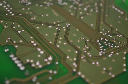
The pad, basic unit of surface mount assembly, is used to pattern PCB pads, i.e. different combinations of pads designed for special types of components.
Gaskets are used to electrically connect, secure a device, or are part of conductive pattern of both.

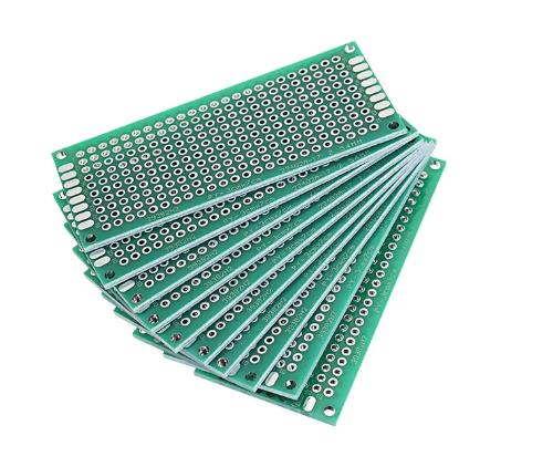
Types of PCB pads
1. Shared pads
1. Square pad - often used when components on PCB are large and few, and the printed wires are simple. When making a printed circuit board by hand, this pad is easy to use.
2. Round pads are widely used in single- and double-sided printed circuit boards with a regular arrangement of components. If density of board allows, then pad can be made larger so that it does not fall off when soldering.
3. Island-shaped platform - lining and connection between linings are combined into one. It is often used in an irregularly shaped vertical installation.
4. Polygonal Gaskets - Used to distinguish between gaskets with same outer diameter but different holes, which is convenient for processing and assembly.
5. Oval pad. This type of spacer has sufficient area to improve stripping protection capability and is often used in double row applications.
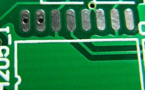
6. Open shape pad - to ensure that hole of pad during manual repair soldering is not sealed with solder after soldering with a solder wave.
Second, special rug
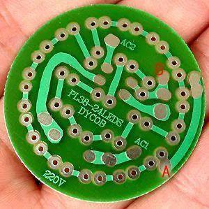
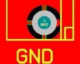
1. Plum blossom
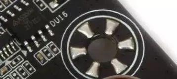
Plumblossom pads are commonly used at ground locations for large vias. There are several reasons for this:
1) The mounting hole must be plated and connected to GND. If mounting hole is fully plated, it is easy to block during reflow soldering.
2) Using internal metal screw holes may result in a poor grounding condition due to reasons such as installation or repeated disassembly. Using plum blossom pads can provide good grounding regardless of load changes.
2. Cushion for flowers
Cross color pads are also called thermal pads, hot air pads, etc. Its function is to reduce heat dissipation of pad to outside during soldering, so as to prevent false soldering or PCB peeling caused by excessive heat dissipation.
1) When your pad is sharpened. The cross flower can reduce ground wire connection area, slow down heat dissipation rate, and facilitate welding.
2) When your PCB needs to be machine mounted and is a reflow soldering machine, cross pad can prevent PCB from peeling off (because more heat is needed to melt solder paste).
3. Drop pillow
It is often used when tracks connected to pads are thin, to prevent pads from peeling off and tracks from pads coming off. This pad is commonly used in high frequency circuits.
Pad Design Standards for PCB Design
1. PCB pad shape and size design standards:
1. Calling library of standard PCB packages.
2. The minimum side of platform on one side is not less than 0.25 mm, and diameter of entire platform is not more than 3 times diameter of component hole.
3. Try to keep distance between edges of two pads greater than 0.4 mm.
4. Pads with a bore diameter greater than 1.2 mm or a pad diameter greater than 3.0 mm shall be diamond or plum shaped.
5. In case of dense wiring, it is recommended to use oval and oblong grounds. The diameter or minimum width of a single-sided contact pad is 1.6 mm; pad of low-current line of double-sided board only needs to add 0.5mm to hole diameter, and pad is too large to cause unnecessary continuous welding.
Second, PCB pad through standard hole size:
The inner hole of shoe is usually not less than 0.6mm, because hole smaller than 0.6mm is not easy to process when stamping. Usually, diameter of metal pin plus 0.2mm is used as diameter. inner hole of pad, for example, metal of resistor. When pin diameter is 0.5mm, diameter of inner hole of pad is 0.7mm, and diameter of pad depends on diameter of the inner hole.
Third, PCB design reliability:
1. Symmetry To balance surface tension of molten solder, pads at both ends must be symmetrical.
2. Pad spacing: If pad spacing is too large or too small, it may cause soldering defects, so make sure distance between terminals or pins of component and pads is correct.
3. The remaining dimension of pad, remaining dimension after end of component or pin overlaps with pad, must ensure that solder joint can form a meniscus.
4. The width of pad should be basically same as width of end or pin of component.
Related
- How many types of pads have you seen in PCB design?
- A list of most common PCB design mistakes, see how many mistakes have you made?
- How many of these free and easy to use circuit design programs have you used?
- Do you know layout requirements of some special devices in PCB design?
- In circuit design, what are differences between six types of grounds?
- How to make anti-interference PCB design?
- 44 types of practical schemes, you will master, you will know everything!
- What does inside of a multilayer PCB look like? Three-dimensional general analysis of design process of high-quality printed circuit boards
- Explain in detail classification of more than a dozen types of "recommended collection" capacitors
- Switching Power Supply PCB Design Skills
Hot Posts
 How to distinguish induction from leakage, we will teach you three tricks! Ordinary people can also learn super practical
- What is drowning in gold? Why Shen Jin?
- This is a metaphor for EMI/EMS/EMC that can be understood at a glance.
- How many types of pads have you seen in PCB design?
- Summary of Common PCB Repair Techniques
- What is three anti-paint? How to use it correctly?
- Knowing these rules, you will not get confused looking at circuit diagram.
- How to make anti-interference PCB design?
- Can diodes do this?