Location:Home Page > Archive Archive
What does inside of a multilayer PCB look like? Three-dimensional general analysis of design process of high-quality printed circuit boards
2023-03-18【Archive】
When hardware engineers first encountered multilayer printed circuit boards, they were easily dizzy. There are often ten or eight floors and queues are like cobwebs.
Today, draw some diagrams of internal structure of multilayer PCBs and use 3D graphics to show internal structure of PCB circuits with different stack structures.
01
Vias are foundation of HDI
Processing a multi-layer circuit board is no different from processing a single-layer and double-layer printed circuit board. The biggest difference is in through hole process.
All lines are etched and vias are drilled and copper plated. Everyone involved in hardware development understands this, so I won't go into details.
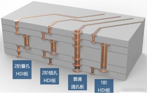
Multilayer printed circuit boards typically include thru-hole boards, first-order boards, second-order boards, and stacked-hole second-order boards. Higher-level boards, such as third-order boards and any level of interconnect boards, are rarely used and expensive, so we won't discuss them here.
Typically, 8-bit microcontroller products use dual-layer through-hole boards; smart hardware at 32-bit MCU level uses 4-layer-6 through-hole boards. fees; intelligent hardware at level of Linux and Android, use 6 layers through holes for 8 first-order HDI boards; compact products such as smartphones typically use 8 layers of first order per 10-layer second stage PCB.

8-layer dual-stage vias, Qualcomm Snapdragon 624
02
Most common transitions
There is only one type of transition from first layer to last. Regardless of whether it is an external or internal contour, holes are punched through, which is called a through plate.
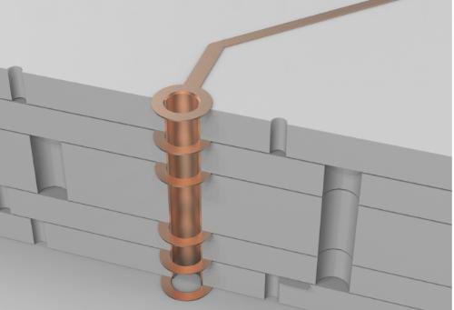
Through-hole boards have nothing to do with number of layers, usually two-layer boards used by everyone are through-hole boards, and many switches and military PCBs have 20 layers, and they are still through boards.
Use a drill to drill through PCB and then copper plate hole to form a through hole.
It should be noted that through hole IDs are typically 0.2mm, 0.25mm and 0.3mm, but typically 0.2mm is much more expensive than 0.3mm. Because drill is too thin and easy to break, drill is slower. The time spent and cost of drill are reflected in increase in price of printed circuit board.
03
Laser Hole for High Density Board (HDI Board)
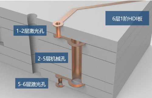
This image shows block diagram of a 6-layer, single-stage HDI board. Two layers on surface are laser holes with an inner diameter of 0.1 mm. The inner layer is a mechanical hole, equivalent to a 4-layer plate with through holes, and outer layer is covered with 2 layers.
Laser can only penetrate fiberglass plate, not copper metal. Therefore, punching holes on outer surface will not affect other internal circuits.
After laser drilled hole, copper was plated to form hole for laser.
04
2-Stage HDI Board with 2 Layers of Laser Holes
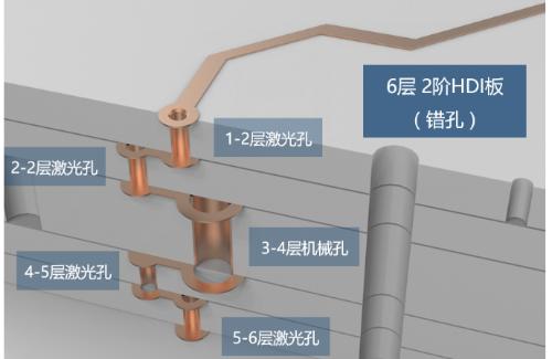
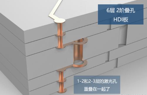
This image shows a 6-layer 2-stage HDI board with offset holes. Usually people use 6 floors and 2 floors and most of them start with 8 floors and 2 floors. There are more layers here, that is 6 layers.
The so-called 2nd order means there are two layers of laser holes.
The so-called irregular hole means that two layers of laser holes are staggered.
Why stagger? Since there is not enough copper plating, hole is empty, so you can't drill holes directly on it, you have to go a certain distance, and then make a layer of holes.
6 floors of second stage = 4 floors plus 2 floors outside first stage.
8 floors of second stage = 6 floors plus 2 floors outside first stage.
05
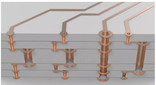
A plate with holes in a stack is more difficult and expensive
The two layers of laser holes in offset hole plate overlap. The queue will be tighter.
It is necessary to galvanize and fill laser hole of inner layer, and then make laser hole of outer layer. The price is more expensive than wrong hole.
06
Super-expensive multi-layer backplane with multi-layer laser holes
That is, each layer is a hole for laser, and each layer can be connected together. You can route wires way you want and make holes way you want.
Linkers think it's cool! Never be afraid that you won't be able to draw anymore!
Buying makes me cry just thinking about it, it's more than 10 times more expensive than regular pass-through boards!
So, only products like iPhone are ready to use it. As for other brands of mobile phones, I have never heard of anyone using any kind of backplane layer.
Overview
Place image at end and compare it carefully.
Please pay attention to size of hole and whether hole platform is closed or open.
Related
- What does inside of a multilayer PCB look like? Three-dimensional general analysis of design process of high-quality printed circuit boards
- Analysis of power circuit of a classic single-chip microcomputer
- Analysis of damping RC circuit of a switching power supply "haberdashery"
- Experience in recognition of circuit diagrams of electronic circuits and method of circuit analysis
- Analysis of various losses inside a switching power supply from 4 aspects
- What is a delay scheme? Explanation of 6 Kinds of Delay Circuit Principles
- In circuit design, what are differences between six types of grounds?
- Principal analysis of BUCK / BOOST circuit, a summary is also in place
- Haberdashery|General failure mechanism and analysis of electronic components
- A list of most common PCB design mistakes, see how many mistakes have you made?
Hot Posts
 How to distinguish induction from leakage, we will teach you three tricks! Ordinary people can also learn super practical
- What is drowning in gold? Why Shen Jin?
- This is a metaphor for EMI/EMS/EMC that can be understood at a glance.
- How many types of pads have you seen in PCB design?
- Summary of Common PCB Repair Techniques
- What is three anti-paint? How to use it correctly?
- Knowing these rules, you will not get confused looking at circuit diagram.
- How to make anti-interference PCB design?
- Can diodes do this?