Location:Home Page > Archive Archive
A list of most common PCB design mistakes, see how many mistakes have you made?
2023-03-18【Archive】
Mistakes are inevitable in process of designing hardware circuits. Listed below are five of most common design problems and corresponding countermeasures in PCB design.
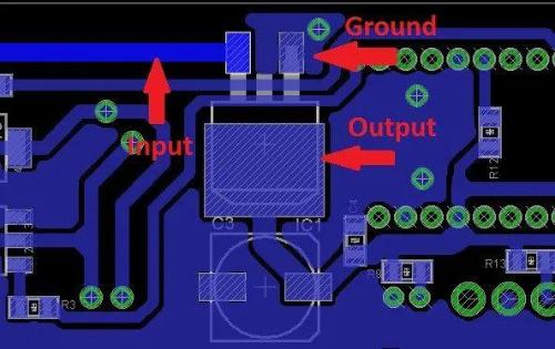
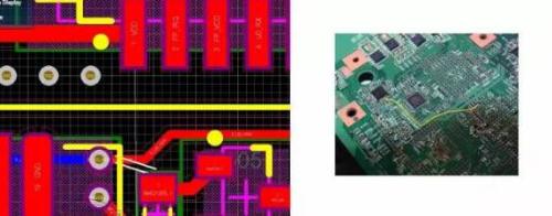
PIN error
A series linear regulated power supply is cheaper than a switching power supply, but power conversion efficiency is low. Generally, many engineers prefer to use linear regulated power supplies due to their ease of use and affordability.
However, it should be noted that although it is convenient to use, it consumes a lot of power and causes a lot of heat dissipation. In contrast, switching power supplies are more complex but more efficient.
However, it should be noted that output pins of some regulated power supplies may not be compatible with each other, so you should check corresponding pin definitions in IC manual before connecting.
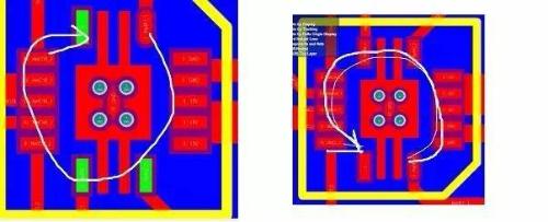
Wrong wiring
Comparative inconsistencies between design and layout are main mistakes made in final stages of PCB design. So some things need to be checked.
For example, device size, quality, tablet size, view level, etc. In short, re-checks are needed to make sure design layout is correct.
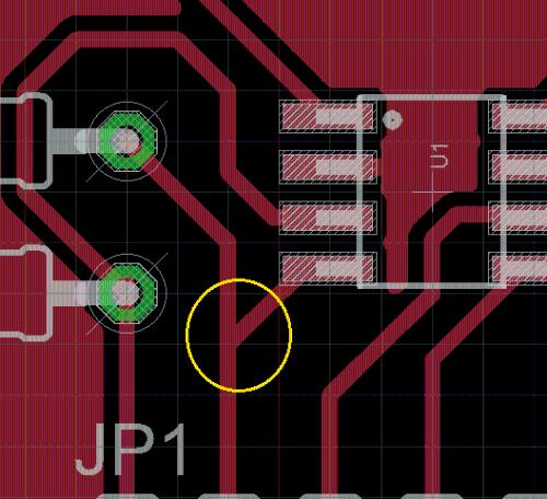
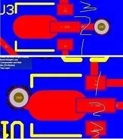
Corrosion Trap
When angle between PCB pins is too small (acute angle), corrosion traps (acid traps) can form.
These sharp joints can remain in corrosive solution during PCB corrosion stage, thereby removing more of copper plating in place, thereby creating stuck spots or traps.
At a later stage, wire may be broken, resulting in an open circuit. Through the use of photosensitive pickling solutions in modern manufacturing processes, this corrosion trap phenomenon has been greatly reduced.
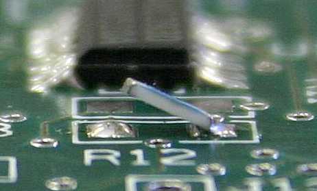
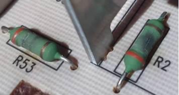
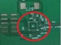
 Tombstone Devices Welding Some Small Devices Surface Mount Devices , solder penetration will cause a one-sided deformation in device, commonly known as "tombstone".
This phenomenon is usually caused by an asymmetrical wiring pattern, which results in uneven heat distribution across surface of device. Tombstone can be effectively reduced with proper DFM checks.
 Lead Width
When PCB lead wire current exceeds 500mA, capacity of first PCB wire diameter will not be enough. At typical thicknesses and widths, wires on a PCB surface carry more current than wires inside a multilayer PCB because surface leads can dissipate heat through airflow.
The line width is also related to thickness of copper foil on layer. Most PCB manufacturers allow a choice of copper foil thicknesses from 0.5 oz/sqft to 2.5 oz/sqft.

Here are some mistakes you can make if you're not careful:
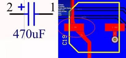
1. Do capacitors with polarity reverse contacts on circuit diagram and PCB?
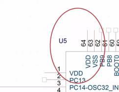
2. Forgot to connect power and ground. . . . There is also opposite. . .
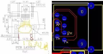
3. Connector string sequence reversed
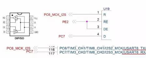
4. RX and TX are swapped. . .
5. Write a package as a matter of course, but there is no device with that specification. Baidu Wenku downloaded datasheet, but it turned out that this device cannot be bought at all.
6. Copy schematic directly, but device can't be bought at all.
Earlier, a team worked on smart locks, and scheme directly copied Samsung smart locks. As a result, a capacitive touch controller was made in Korea, which was difficult to buy, and there was no agent or support service. . Just experiment and explore for yourself.
7. When choosing a capacitor, only capacitance is taken into account, and withstand voltage is not taken into account. As a result, such a large package cannot accommodate a capacitor that meets specifications.
8. When choosing a resistor, look only at resistance value, not power consumption.
9.After drawing PCB, don't look at DRC report, just look at flying wires with your eyes. After returning to board, flying wires will actually fly.
10. The packaging is upside down. . .
11. The solder mask layer of heat dissipation pad is unfinished
Related
- A list of most common PCB design mistakes, see how many mistakes have you made?
- How many types of pads have you seen in PCB design?
- Common Mistakes of Electronics Engineers
- How many of these free and easy to use circuit design programs have you used?
- Do you know layout requirements of some special devices in PCB design?
- Summary of Common PCB Repair Techniques
- How to make anti-interference PCB design?
- What does inside of a multilayer PCB look like? Three-dimensional general analysis of design process of high-quality printed circuit boards
- What is a magnetic sensor? The most common types of magnetic sensors and their applications
- A Few Design Tips PCB Engineers Need to Know
Hot Posts
 How to distinguish induction from leakage, we will teach you three tricks! Ordinary people can also learn super practical
- What is drowning in gold? Why Shen Jin?
- This is a metaphor for EMI/EMS/EMC that can be understood at a glance.
- How many types of pads have you seen in PCB design?
- Summary of Common PCB Repair Techniques
- What is three anti-paint? How to use it correctly?
- Knowing these rules, you will not get confused looking at circuit diagram.
- How to make anti-interference PCB design?
- Can diodes do this?