Location:Home Page > Archive Archive
Do you know layout requirements of some special devices in PCB design?
2023-04-01【Archive】
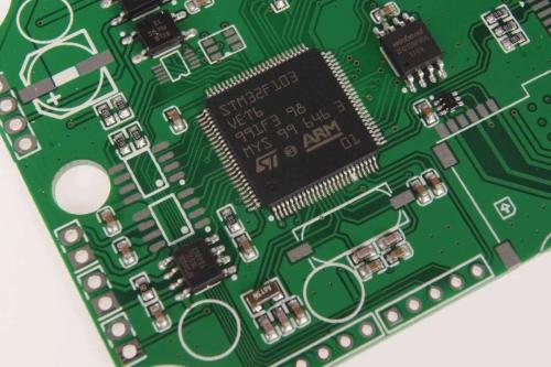
The layout of a device on a printed circuit board is not arbitrary, it has certain rules that everyone must follow. In addition to general requirements, some special devices also have different layout requirements.
Compression Component Layout Requirements
1) There must be no components higher than 3mm within 3mm of bent/male and bent/female surfaces of crimp, and no soldering tools within 1.5mm around; There should be no components within 2.5mm of center of hole.
2) Straight/male and straight/female crimps must be free of components within 1mm; when it is necessary to install a sheath on back of straight/male and straight/female crimps, it cannot be within 1mm of edge of sheath Locate any components, and no components should be within 2.5mm of crimp hole when sheath is not installed .
3) For live plug of grounding plug used with European plug, front end of long pin is 6.5mm and short pin is 2.0mm.
4) The long pin of 2mm FB power supply single pin pin matches 8mm barring at front end of single board connector.
Requirements for placement of temperature-sensitive devices
1) When placing devices, temperature-sensitive devices (such as electrolytic capacitors, crystal oscillators, etc.) should be kept as far away from high-temperature devices as possible.
2) The temperature sensing device must be close to component under test and kept away from high temperature areas so that it is not affected by other equivalent components that generate heat and cause malfunctions.
3) Place heat-producing and heat-resistant devices near air outlet or at top, but if they cannot withstand higher temperatures, they should also be placed near air inlet, while making sure that they are as close as possible to other devices, heat generating and heat sensitive devices.
Polarity device layout requirements
1) THD devices with polarity or directivity are aligned in same direction in layout and arranged neatly.
2) The direction of polarized SMCs should be as consistent as possible on board, devices of same type should be placed neatly and nicely.
(Devices with polarity include: electrolytic capacitors, tantalum capacitors, diodes, etc.)
Planning requirements for through-hole reflow soldering devices
1) For PCBs with a non-transmitting side dimension greater than 300mm, avoid placing heavier components in middle of PCB to reduce effect of weight of inserted components on PCB deformation during welding. process and effect of insertion process on PCB The effect of components already placed on board.
2) For convenience of plug-in, it is recommended to place device next to side of plug-in.
3) It is recommended that length direction of devices with large dimensions (such as memory slots, etc.) match transmission direction.
4) The distance between pad edge of through-hole reflow device and QFP, SOP, connector, and all BGAs with a pitch of ≤0.65mm exceeds 20mm. Distance from other SMT devices > 2 mm.
5) The distance between body of through-hole reflow soldering device is > 10 mm.
6) The distance between pad edge of through-hole reflow device and transmitting side is ≥ 10 mm, distance from non-transmitting side is ≥ 5 mm.
Related
- Do you know layout requirements of some special devices in PCB design?
- How many types of pads have you seen in PCB design?
- PCB design guidelines: safety regulations, layout and wiring, EMC, thermal design, process engineering.
- Do you know 4 characteristics of Schottky diodes?
- Diagram of relationship between PCB layout and EMC
- A list of most common PCB design mistakes, see how many mistakes have you made?
- A Few Design Tips PCB Engineers Need to Know
- "Jingzhen" stroked you: "Do you know how I work?"
- Should PCB trace angle be 90°? — Jumping guide to PCB layout pit
- PCB puzzle, these few special rules!
Hot Posts
 How to distinguish induction from leakage, we will teach you three tricks! Ordinary people can also learn super practical
- What is drowning in gold? Why Shen Jin?
- This is a metaphor for EMI/EMS/EMC that can be understood at a glance.
- How many types of pads have you seen in PCB design?
- Summary of Common PCB Repair Techniques
- What is three anti-paint? How to use it correctly?
- Knowing these rules, you will not get confused looking at circuit diagram.
- How to make anti-interference PCB design?
- Can diodes do this?