Location:Home Page > Archive Archive
(Detailed detailed text) 60 pictures step by step analyze PFC power supply designed by UC3854.
2023-12-04【Archive】

01 Power Factor Correction (PFC)
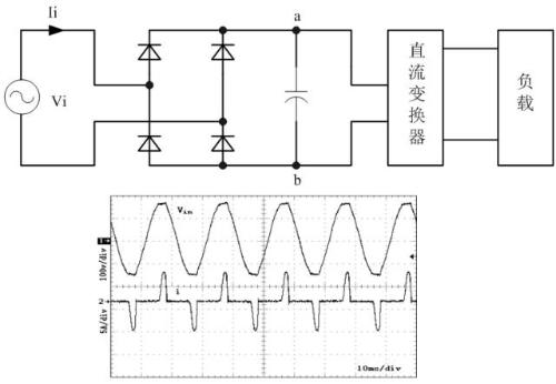
In traditional AC-to-DC and switching power supplies, input circuit usually uses a diode bridge rectifier, and output terminal is directly connected to a large capacitance filter.
Although uncontrolled rectifier circuits are simple and reliable, they generate high peak currents that distort input current waveform, reducing AC power factor to 0.5~0.65 and causing excessive reactive power losses. So we have to introduce power factor correction.
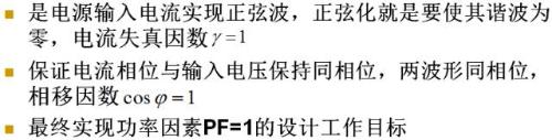
Determination of power factor
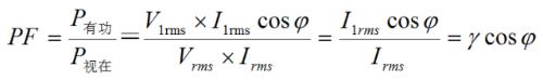
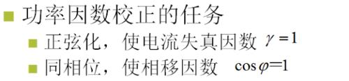
Power factor correction Power factor correction has been a major area of power technology development for more than a decade. Its main principle is:
Two main methods of power factor correction
1) Passive PFC
2) Active PFC technology
Single-tube power factor correction converter concept
Using only one main switching lamp, it is possible to correct power factor above 0.8 and adjust the DC output voltage. This topology is called single lamp single stage power factor converter.
Single-tube power factor correction converter circuit type
Tank
Zoom
Acceleration
Zeta
Cook
Sepik
02 PFC converter based on Boost circuit and control method
Power Factor Correction (PFC)
PFC converter proposal based on boost circuit

Boost benefits for PFC:
1.Boost can work in three modes: CCM, BCM and DCM;
2. The energy storage inductor is also a filter, which can suppress EMI and RFI interference, and current waveform distortion is small;
3. High output power;
4. The common source can simplify control scheme and other advantages.
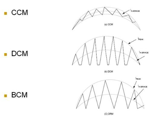
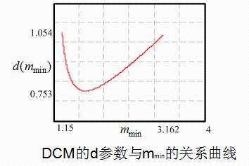
PFC boost converter and its control method - DCM
DCM
Suppose that under steady-state conditions during a switching cycle, conduction time of MOSFET is Ton, input voltage is Ui, inductor current is i, peak inductor current is imax, inductance is L, and inductor current reaches its peak value corresponding to input voltage is . Then, during conduction period of MOS tube, following occur:
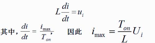
If duty cycle of each switching cycle in input cycle is approximately constant, peak inductor current is proportional to input voltage. Thus, waveform of input current naturally follows waveform of input voltage, and circuit can realize PFC function without a current control loop.
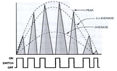
Key to DCM
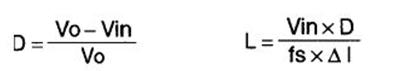
To ensure that a circuit is discontinuous over a certain voltage range, key is to calculate inductance. The final formula for calculating the inductance is given below:
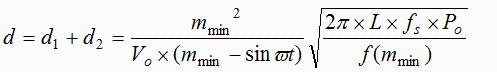
d1 is MOSFET conduction duty cycle, d2 is freewheel conduction duty cycle, L is inductance, fs is switching frequency, Po is output power, and mmin is Vo/Vin.

To ensure that inductor current is discontinuous, condition d1+d2<1;
As mmin=Vo/Vin d1+d2 increases, it first decreases and then increases, so when input voltage is low or high, inductor current tends to be continuous.
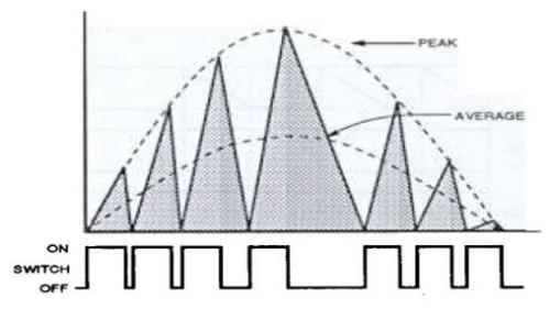
PFC converter based on Boost circuit and control method - BCM
BKM
Usually, frequency conversion control is used. Under condition of a fixed power-on time, turn-off time is adjusted so that inductor is always in critical conduction mode, and unity power factor can be obtained, which is suitable for low to medium power applications. The switching frequency is not fixed (frequency conversion), and conduction time of power tube is fixed.
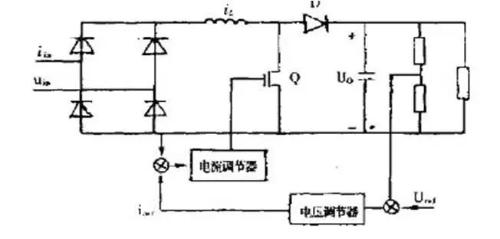
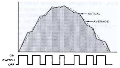
PFC converter based on Boost scheme and its control method - CCM
Overview
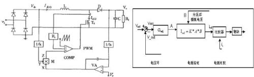
Typically, continuous current inductor control circuit should have an analog multiplier and a current detection circuit to modulate control signal of power switch tube, together with output voltage feedback signal and accuracy of analog multiplier will affect power factor value and harmonic content of input current THD. The schema looks like this:
Control mode in CCM state
1. Peak current control;
2. Average current control;
3. Hysteresis control;
4. Single loop control.
SKK
When inductor current is continuous, you can choose a variety of control methods, such as: peak current control, hysteresis current control, average current control, single cycle control, etc., suitable for high power occasions, and switching frequency can be constant (for example, average current control, etc. (fixed frequency)), and can also be changed (for example, hysteresis control (frequency conversion)).
PFC converter based on Boost circuit and its control method - summary
DCM
The input current automatically tracks input voltage, control is simple, only one voltage loop is required, low cost, low inductance, ZCS supervisor, freewheel has no reverse recovery problems, and operates at a fixed frequency, suitable for low-power electrical equipment.
BKM
The input current automatically tracks input voltage, inductance is small, and frequency conversion control is generally used. Under condition of a fixed power-on time, adjust power-off time so that inductance is always critical conduction mode and power of unit can be obtained by factor, but filter design is complex, suitable for low to medium power applications.
SKK
The commonly used methods are peak current control method, current hysteresis control method or average current control method, which can be fixed or variable frequency, high power factor, multiplier is used, the control is relatively complicated and expensive. . Suitable for high power occasions.
PFC control method—CCM-Peak Current Control
1. Peak current monitoring
The basic block diagram of peak current control is as follows:

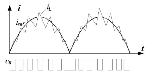
• When inductor current reaches reference current, switch is always on;
• The reference current is determined by product of sampling value of full-wave rectified voltage and output signal of voltage loop error amplifier. Once inductor current reaches reference current, comparator outputs a trip signal to open circuit breaker; switch is again turned on by clock at a fixed frequency, so that periodic changes occur; • The peak current envelope of inductor follows waveform of rectified voltage Vdc so that input current and input voltage of voltage have same phase and are close to a sinusoid.
Summary
The advantage of peak current control is that it is easy to implement, but disadvantage is that when AC mains voltage changes from zero to peak, its duty cycle changes from its maximum value (usually 95%) to its minimum. value (near mains peak voltage). When duty cycle is > 50%, current loop will create sub-harmonic oscillations, which often occur in constant frequency PWM DC-DC converters, so this phenomenon will also take place in this circuit. To overcome this phenomenon, a slope compensation function must be added to comparator input, but sometimes it is still not ideal even after slope compensation.
2. Medium Current Control
The basic block diagram of average current control is as follows:
Average current monitoring benefits:
The current loop has a higher bandwidth;
Minor tracking error;
Transient response is better;
THD(<5%) and EMI are small;
Not sensitive to noise;
Fixed switching frequency is suitable for high power applications and is currently most widely used PFC control method.
3. Current control with hysteresis
The basic block diagram of hysteresis current control is as follows:
The function of external voltage loop is to provide an instantaneous current reference to hysteresis control unit as an input to hysteresis logic controller.
After detected input voltage is divided, two reference currents are generated: an upper limit and a lower limit.
When inductor current reaches reference low limit, switch tube turns on and inductor current increases. When inductor current reaches reference high limit, switching tube turns off and inductor current drops.
The width of current hysteresis loop determines size of current ripple, and switching frequency is determined by width of loop (frequency conversion).
Advantage
The capacity of current loop is high;
It has high reliability and fast dynamic response;
Minor current tracking error;
The hardware implementation is simple.
Disadvantages
The magnitude of load has a great influence on switching frequency;
This does not contribute to development of optimal design of output filter. At present, research to improve hysteresis current control circuit is still very active. The goal is to realize constant frequency control (by changing loop width in real time) Combined control is one of development directions.
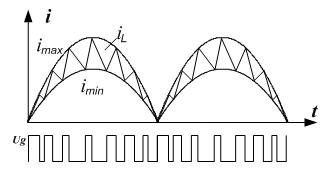
4. Single cycle control
Single-cycle control is a new type of non-linear control strategy pioneered in BUCK converters.
When input or output signal jumps, single-ended control can achieve control target in one switching cycle, which greatly improves dynamic performance of system, and extends to various applications such as power factor correction, active filter, rectifier, etc., etc. e.
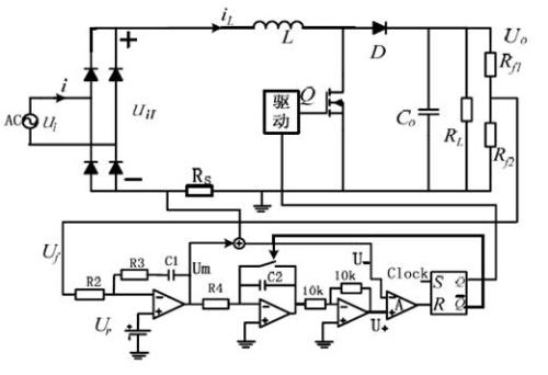

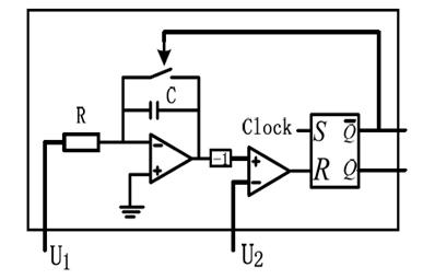
Single-cycle control is a control method that does not require a multiplier, but instead has a reset integrator, as shown in figure above. The RC time constant is equal to RS flip-flop clock cycle, so relationship is:
d is integral duty cycle.
The purpose of power factor correction is to ensure that input current matches input voltage and equivalent resistance of converter is linear. Yes:
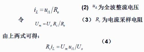
If output filter capacitor is large enough, output voltage Uo can be considered as a constant value, and it can be seen that Um can also be considered as a constant value in one switching cycle.
So it can be seen from (4) that Boost input current is proportional to input voltage in order to achieve target of current tracking voltage.
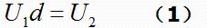
In one switching cycle, ratio between boost converter output voltage and input voltage is:
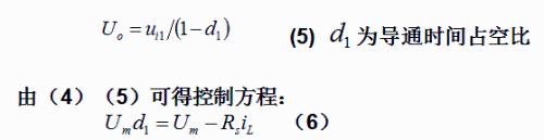
If U1=Um, U2=Um-RsiL, goal of control can be achieved with control scheme!
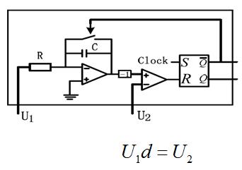
Single loop control scheme is shown in figure below:

Reset integrator as shown:
Benefits;
Weekly monitoring can optimize system response;
Reduce distortion and suppress power noise;
Quick reply;
Constant switching frequency
High reliability;
Easy to implement;
Anti-jamming control scheme is simple;
PFC Control Method - CCM Summary
Overview of control strategy in CCM mode
(1) Peak current control: The advantage is that it is easy to implement, but disadvantage is that when AC mains voltage changes from zero to peak, duty cycle changes too much. When duty cycle is > 50%, current loop will produce sub-harmonic oscillations.
(2) Average current control: advantage is that current loop has large bandwidth, small tracking error, good transient response, low non-linear distortion (<5%) and electromagnetic interference, noise insensitivity, fixed switching frequency , is suitable for high power applications, and its disadvantage is that error between reference current and actual current changes with duty cycle, which can generate low-order current harmonics.
(3) Hysteresis current control: The advantages are high current loop capacity, high reliability and fast dynamic response capability, small current tracking error, and easy hardware implementation. Its disadvantage is that magnitude of load has a large influence on switching frequency, which does not contribute to optimal design of output filter.
(4) Single-ended control: It can optimize system response, reduce distortion, and suppress power supply interference. It has advantages of fast response, constant switching frequency, high reliability, easy implementation, power supply anti-interference and simple control circuit. .
The main ways to deal with harmonic pollution:
Passive line filter (PPF)
Active power filter (APF)
Active power factor correction (APFC) based on Boost PFC
DCM
BKM
SKK
Average current control
Peak current monitoring
Hysteresis control
Single control loop
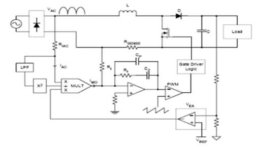
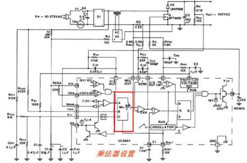
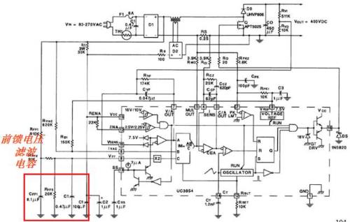
03 Introduction to UC3854, a typical PFC chip
Introduction to UC3854, typical PFC overview
UC released UC3854 in late 1994.
Together with Unitrode, Motorola, Silicon, Siemens and other companies, released various active power factor correction chips, such as UC3852, UC3854, 3854AB, UC3855, MC34261, ML4812, ML4821, TDA4814, etc., single-phase active power factor . Correction technologies are developing rapidly.
UC3854 provides active power factor correction for power supply. It can limit non-sinusoidal current change according to sinusoidalmains voltage. The device can make best use of supply current to minimize mains current distortion and perform all PFC functions.

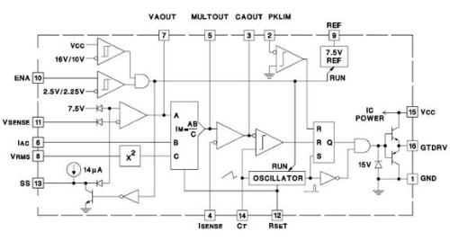
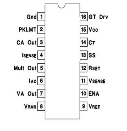
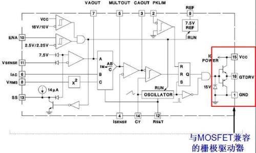
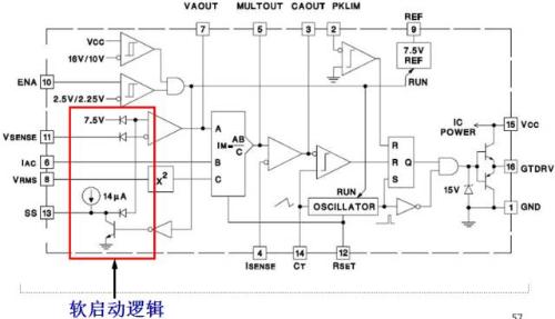
Introduction to a typical UC3854 PFC chip - function of each pin
The function of each UC3854 pin:
Pin 1 (Gnd): All voltage measurements refer to ground level at Gnd pin.
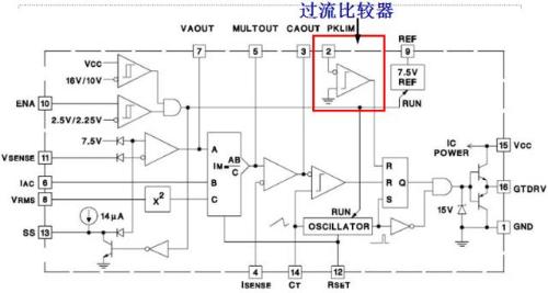
Pin 2 (PKLMT): peak current limiting contact.
Pin 3 (CAOut): current error amplifier output pin.
Pin 4 (Isense): current error amplifier inverting input
Pin 5 (MultOut): multiplier output and current error amplifier positive input.
Pin 6 (Iac): AC input.
Pin 7 (VAOut): Voltage amplifier output. Pin 8 (Vrms): Mains voltage rms value terminal.
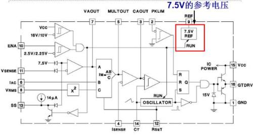
Pin 9 (Vref): voltage reference output.
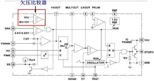
Pin 10 (ENA): enable control terminal.
Pin 11 (Vsense): voltage amplifier inverting input.
Pin 12 (Rset): generator charging current setting and multiplier current limit
Pin 13 (SS): soft start terminal.
Terminal 14 (Ct): generator capacitor setting terminal.
Pin 15 (Vcc): supply voltage positive polarity.
Pin 16 (GTDrv): shutter drive.
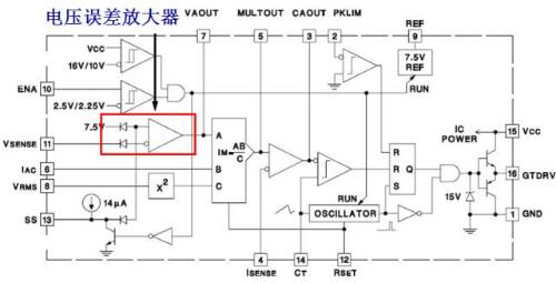
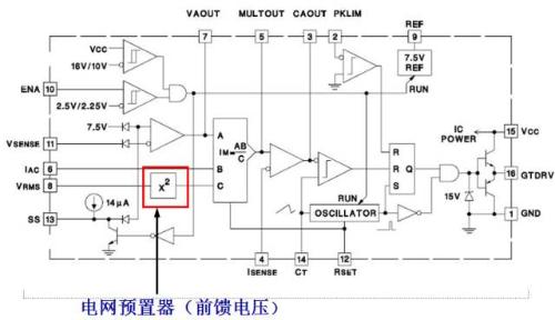
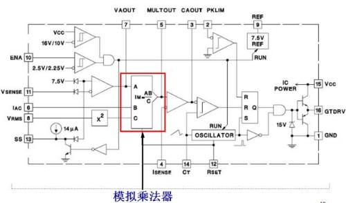
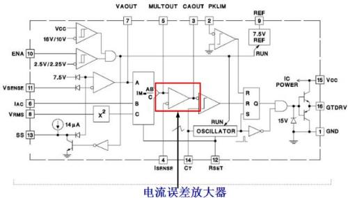
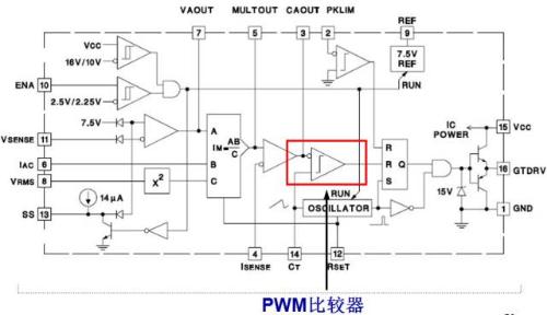
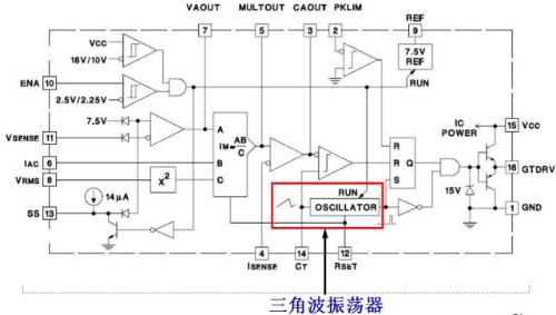
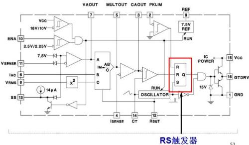
Introduction to UC3854, typical composition of PFC chips
Voltage Error Amplifier
Network Preset (Feedforward Voltage)
Analogue multiplier
Current Error Amplifier
Triangle wave oscillator
PWM comparator
RS Trigger
MOSFET compatible gate driver
Reference voltage 7.5V
Undervoltage comparator
Overcurrent comparator soft start logic
Introduction to UC3854, a typical internal structure of a PFC chip
Introduction to UC3854, typical PFC chip performance
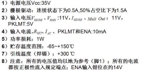
UC3854 key features:
Suitable for Boost scheme
Suitable for CCM mode
Average current control
Constant switching frequency up to 200 kHz
Maximum duty cycle is 95%.
Single signal output
Drive output voltage 14.5V, drive output current 1A
Soft start
Input power undervoltage protection
Output overload protection function
UC3854 design features
1) Set power factor to 0.99
2) Limit current distortion in the network <5%
3) Suitable for global mains voltage (AC 80~270V)
4) Predictive grid voltage regulation, low noise, high sensitivity
5) Average current mode control
6) Low power supply inrush current, precision reference voltage
7) Fixed Frequency Pulse Width Modulation (PWM)
8) Low Offset Analog Multiplier
9) 1A Gate Driver
Introduction to a typical PFC UC3854 chip - operating conditions
Optimal working conditions UC3854
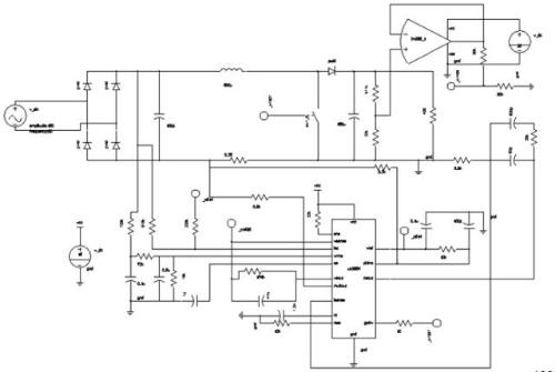
Introduction to a typical PFC UC3854 chip - power stage application
The control circuit of boost power factor corrector PFC almost does not change depending on power of converter.
Generally, 500W PFC is basically same as 50W PFC control circuit, only power circuit is different, but control circuit design steps are basically same.
An example of a PFC converter design based on a step-up circuit
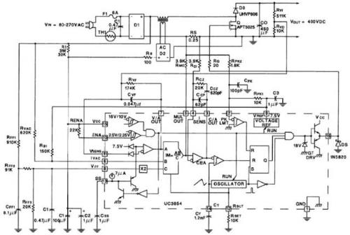
1. Design Indicators
Input voltage: AC 80-270V
Input frequency: 45Hz~65Hz
DC output voltage: 400 VDC
Output power: 250W
Power factor: >98%
Input current THD: <5%
2. Switching frequency
Usually, switching frequency can be chosen arbitrarily, but it must be high enough to miniaturize power circuit, reduce distortion, and maintain high conversion efficiency. In most applications, a switching frequency range of 20 to 300 kHz is an acceptable compromise. As a compromise between size and efficiency, this example uses a switching frequency of 100 kHz. In addition, value of inductance should be small enough to keep distortion peak in minimum range, amount of inductance should be as small as possible, and losses caused by diode should not be too large.

3. Choice of inductance
The inductance value determines total high-frequency ripple current of input, and inductance value can be selected according to set ripple current value △I.
Determining value of inductance starts with peak value of input sinusoidal current, and maximum peak current appears at peak value of minimum mains voltage:
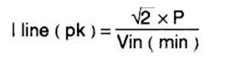
Based on formula above, in this example, power is 250W, minimum mains voltage is 80V, and maximum peak current is 4.42A.
The inductor current ripple is typically chosen to be around 20% of maximum peak current. In this example, maximum peak current is 4.42 A, so peak current ripple is △ I =900 mA.< br>
Vin=1.414×80=113.12 V, fs=100 kHz
Select according to duty cycle voltage and switching frequency here:
From formula above, L=0.89 mH, rounded up to 1 mH.
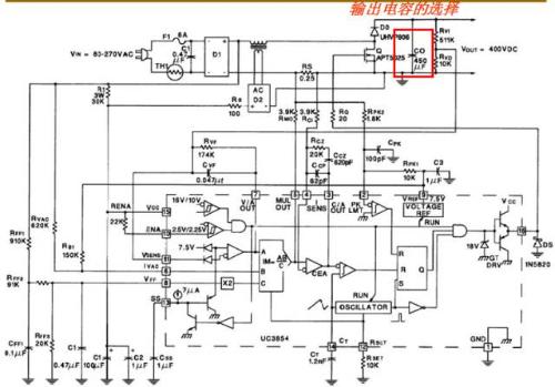
4. Output capacity
The selection factors associated with output capacitor include switching frequency ripple current, secondary ripple current, DC output voltage, ripple output voltage, and hold time. The total current flowing through output capacitor is r.m.s. ripple of switching frequency current and second harmonic of line current. Typically, a large electrolytic capacitor is chosen as output capacitor, and its equivalent series resistance (ESR) varies with frequency (usually very loud at low frequencies). ). Usually, total amount of current a capacitor can handle also depends on temperature rise. As a rule, it is not necessary to calculate exact value of temperature rise, it is sufficient to calculate sum of temperature rise caused by high-frequency pulsating current and low-frequency pulsating current. The data sheet of capacitor contains required ESR values and temperature rises.
In this example, selection of a capacitor is mainly based on hold time. Service time is time that output voltage can remain within specified range after power is removed and is typically 15-50ms. capacitance value per output watt is 1~2uF (empirical value). It can also be determined by following formula (conservation of energy):
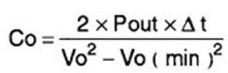
From formula Pout=250W, △t=64ms, Vo(min)=300V, we can calculate that Co=457uF, here we choose 450V 450uF electrolytic capacitor.
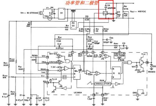
5. Switch lamp and diode
Switches and diodes should be enough to ensure reliable operation of circuit. Generally speaking, rated current of switching tube must be at least greater than peak current of inductor, and rated voltage must be at least greater than output voltage, and diode requirements are same. The diode must be fast to reduce switching losses (the inductor current is continuous, there is a reverse recovery problem).
In this example, diode would be a fast high voltage diode with a reverse recovery time of 35 ns, a breakdown voltage of 600 V, and a forward current rating of 8 A. The power MOSFET has a breakdown voltage of 500 V and a DC current rating of 23 A. this example is mainly caused by reverse diode recovery current.
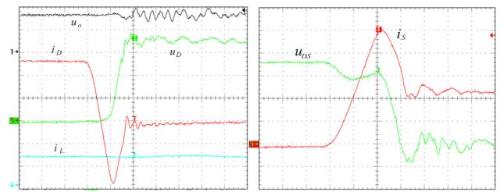
Experimental current and voltage waveforms with diode off and switch on
6. Inductor current detection
Two widely used current detection methods:
(1) Use a measuring resistor between inverter and ground.
(2) Use a current transformer.
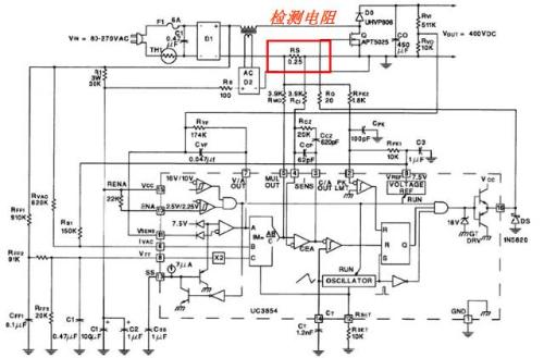
This example uses a current sense resistor to measure current (as shown in figure on page above). The resistance value creates a signal that is strong enough not to be disturbed by noise, yet small. enough not to cause excessive energy loss. A good choice is a detector resistor with a voltage drop of about 1 V. Here, a 0.25 Ω resistor is chosen as Rs. In worst case, a peak current of 5.6A will result in a maximum voltage drop of 1.4V.
7. Peak current limit
The UC3854 peak limit function is activated when instantaneous inductor current exceeds maximum value, i.e. when pin 2 is below ground, switch is turned off. The current limit is set by dividing reference voltage by voltage divider of current measurement resistor:
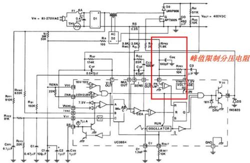
8. Voltage warning signal
VFF is input voltage of quad circuit, and quad circuit of UC3854 typically operates in range of 1.4V to 4.5V. UC3854 has a limit circuit, even if input exceeds this value, rms value of VFF feed forward voltage is limited to 4 .5 V. Direct-coupled input voltage divider has three resistors RFF1, RFF2, RFF3 and two capacitors CFF1, CFF2. Therefore, it can perform two-stage filtering and provide split output voltage. The voltage divider and capacitor form a second-order low-pass filter, so its DC output is proportional to average value of half-sine wave. The average value is 90% of effective value of sinusoidal half wave. For example, ac RMS is 270V, average is 243V, and peak is 382V.
There are two DC conditions that must be met for a VFF feedforward voltage divider. When mains input voltage is high, feed-forward voltage should not exceed 4.5V. When it reaches or exceeds this value, feed-forward voltage will be fixed and feed-forward function will be lost. When mains input voltage is low, voltage divider should be set so that feed-forward voltage is 1.414V. If VFF is less than 1.414V, internal current limiter will keep multiplier output constant.
In this example, divider resistor RFF1 is 910 kΩ, RFF2 is 91 kΩ, and RFF3 is 20 kΩ. When input voltage is 270VAC, average DC is 243V and maximum VFF is 4.76V. When input voltage is 80VAC, average DC is 72V and VFF is 1.41 B.
9. Multiplier settings
The multiplier and divider are basis of power factor corrector. The output of multiplier adjusts current loop to improve power factor of input current. So output of this multiplier is a signal representing input current.
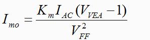
Unlike most design tasks that start from output to input, design of multiplier circuit must start from input. The multiplier has three input terminals: an IAC variable current terminal (pin 6), a VFF input voltage feed-forward terminal (pin 8), and a VVEA output terminal (pin 7) for voltage error amplification. The output of multiplier is current Imo signal (pin 5):

In formula, Km=1 is a constant, IAC is rectified input current, VVEA is voltage error amplifier output, and VFF is feedforward voltage.
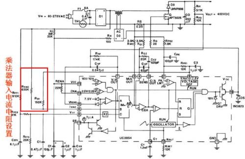
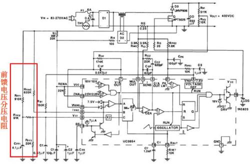
10. Input Current Multiplier
The input current of multiplier depends on input voltage through RVAC. The multiplier has better linearity at higher currents, but recommended maximum current is 0.6 mA. When mains voltage is high, peak voltage is 382V, voltage on pin 6 is 6V, and maximum value obtained with RVAC with a resistance value of 620kΩ is 0.6mA. Since voltage on pin 6 is 6.0V, Bias current is required for circuit to work properly with VIN=0. Connect a resistor Rb1 between VREF reference voltage and pin 6, and IAC can provide minimum bias current, Rb1=RVAC/4, and Rb1 value is 150 kΩ.
11..Output current multiplier
The maximum input current Imo of multiplier is at peak of input sinusoid of lower grid line.
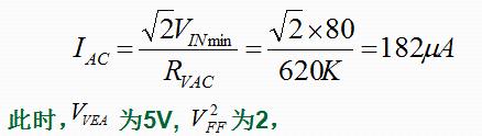
According to above, maximum value of Imo is 365 µA. Imo cannot exceed IAC more than twice.
11. Multiplier output current
The Iset current is another limit for output current of multiplier. Imo cannot be greater than 3.75/RSET. For this example circuit, a maximum value of RSET=10.27 kΩ can be obtained, so 10 kΩ can be chosen.
11. Multiplier output current
To form a current loop feedback loop, output current Imo of multiplier must be added to a current proportional to inductor current to form negative feedback. Resistor Rmo connected between output of multiplier and current sense resistor performs this function, making output of multiplier summing connection of inductor current and current reference.

In this example, above limiting equation is used, inductor peak current is limited to 5.6A, and current sense resistor is 0.25 Ω, so peak voltage across sense resistor is 1.4V. The maximum output current of multiplier is 365 µA, so synthetic resistance Rmo should be 3.84 kΩ, 3.9 kΩ optional.
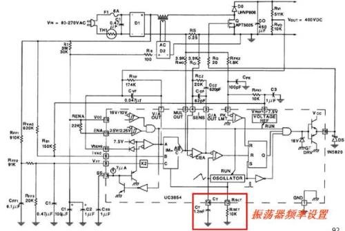
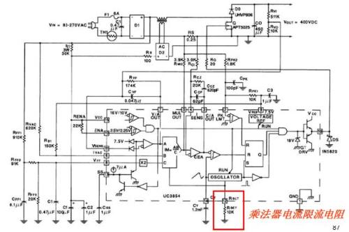
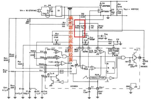
12. Generator frequency
The oscillator frequency is set by capacitor CT and resistor RSET. It is known that resistance RSET is 10 kΩ. The switching frequency fs must be set to 100 kHz. The capacitor is defined by following formula:
So CT is 0.00125uF.
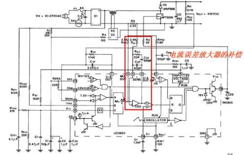
13. Amplifier Error Current Compensation
(1) Calculate voltage drop across detection resistor when inductor current drops, and then divide by the switching frequency. Equation:

Δvrs = (400 × 0.25)/(0.001 × 10,000) = 1.0 V
This voltage should be equal to Vs, which is 5.2V across timer capacitor.
Error amplifier gain:

(2) Feedback resistance, set Rci=Rmo=3.9 kΩ
Rcz=GcaRci=5.2×3.9=20 kOhm
(3) Current loop crossing frequency:

(4) Select Ccz, select a phase range of 45°, and set zero point at loop crossing frequency.
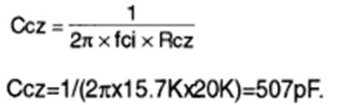
Take 620pF
(5) Select Ccp, pole should be on fs/2,
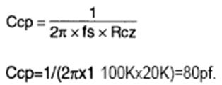
Take 62 pF
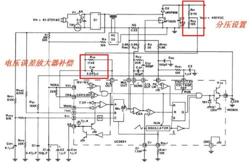
14. Voltage Error Amplifier Compensation
The THD is 5% and 3rd harmonic AC input of 3% is selected as setpoint. 1.5% is assigned to Vff input, 0.75% to output ripple voltage, or 1.5% to Vvac. Leave 0.75% for various non-linear devices.
(1) Output ripple voltage: The output ripple voltage is determined by following formula, where fr is second harmonic frequency:
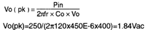
(2) Amplifier gain setting: Vo(pk) should be reduced to ripple voltage allowed by voltage error amplifier output signal, which should set error amplifier gain at 2nd harmonic frequency point, formula is as follows:
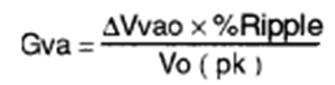
For UC3854 △Vvao is 5-1=4V in example

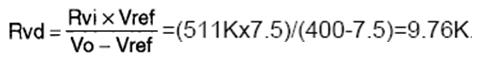
(3) Feedback network value: take Rvi equal to 511

take 0.047uF
(4) Set voltage divider resistor:
take 10 kOhm
(5) Pole frequency:
Boost stage gain:
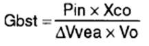
It includes a multiplier, a voltage divider and a quad; Xco is impedance of output capacitor.
At amplifier response poles, gain of the error amplifier is given by:
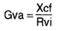
The total voltage loop gain is product of Gbst and Gva and is given by:
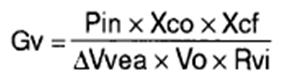
Both Xco and Xcf are frequency related and this function has a power of 2 slope (-40 dB/decade).
To find cutoff frequency, set Gv=1, solve fvi, Xco positioned as 1/(2πfCo), Xcf positioned as 1/(2πfCvf)1/(2πfCo)
The value of Rvf is equal to impedance of Cvf at fvi,
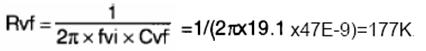
174 kΩ optional
15. Voltage Forward Coupled Filter Capacitor
These capacitors determine 3rd harmonic distortion of Vff distribution at AC input and determine total amount of attenuation required. The content of 2nd harmonic of mains voltage after rectification is 66.2%. THD is allowable percentage of total harmonic distortion.
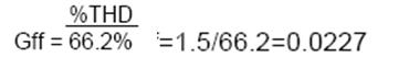
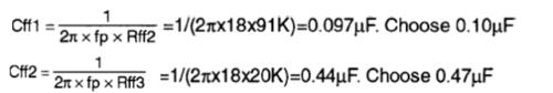
Use two equations to solve poles and find frequency of poles. fr is ripple frequency of second harmonic.
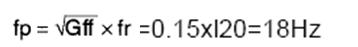
Select Cff1 and Cff2:
UC3854 simulation circuit
UC3854 signal simulation

Current error amplifier output and carrier waveform
Inductor current and drive pulse shape
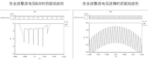
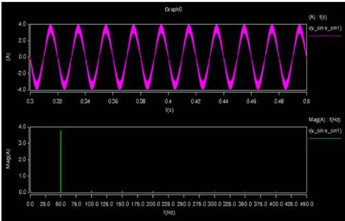
Current signal input and spectrum analysis
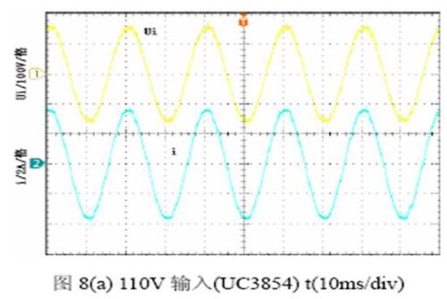
UC3854 experimental waveform
UC3854 Average Current Control Summary
The benefits of this control method:
1 Constant frequency control.
2 Working in continuous state of inductor current, rms value of switching tube current is small, and EMI filter is small.
3 Can suppress switching noise.
4 The waveform distortion of input current is small.
Main disadvantages:
1 The control scheme is complex.
2 Requires multipliers and divisors.
3 It is necessary to determine current of inductor.
4 Current control loop required.
Related
- (Detailed detailed text) 60 pictures step by step analyze PFC power supply designed by UC3854.
- (Detailed long text) Capacitor selection rules in power supply design
- (In-depth long text) Detailed interpretation of switching power supply circuit
- Detailed and detailed explanation of ripple current value of inductance of power supply BUCK r
- Detailed analysis of the "various protection schemes" of a switching power supply
- The composition of switching power supply circuit and a detailed explanation of general circuits
- (Detailed long text) 7 ways to use diodes that engineers need to master
- [Comic] Detailed explanation of knowledge of power sources
- Detailed explanation of commonly used LED drive power
- Detailed analysis of various losses in switching power circuits
Hot Posts
 How to distinguish induction from leakage, we will teach you three tricks! Ordinary people can also learn super practical
- What is drowning in gold? Why Shen Jin?
- This is a metaphor for EMI/EMS/EMC that can be understood at a glance.
- How many types of pads have you seen in PCB design?
- Summary of Common PCB Repair Techniques
- What is three anti-paint? How to use it correctly?
- Knowing these rules, you will not get confused looking at circuit diagram.
- How to make anti-interference PCB design?
- Can diodes do this?