Location:Home Page > Archive Archive
(Detailed long text) 7 ways to use diodes that engineers need to master
2023-04-18【Archive】
Introduction
Many beginners are "familiar" with diodes. When they mention characteristics of a diode, they may blurt out its unidirectional conduction characteristics. When it comes to its application in circuits, first reaction is rectification. They know little about other characteristics and applications of diodes, I also think that by mastering unidirectional conduction of a diode, one can analyze various circuits in which diode is involved. yourself, because this directional thinking affects. In addition to analyzing working principle of various diode circuits, many diode circuits cannot explain their working principles with unidirectional conduction characteristics.
In addition to unidirectional conduction, diodes have many other characteristics. In many circuits, it is not possible to analyze principle of operation of a circuit consisting of diodes using characteristics of unidirectional conduction. More characteristics of diodes need to be mastered to properly analyze them. Circuits such as a simple DC voltage regulator circuit made up of diodes, a temperature compensation circuit made up of diodes, etc.
Simple Diode DC Voltage Regulator Schematic and Troubleshooting
The simple diode voltage regulator circuit is mainly used in some local DC power circuits. Due to simple circuit and low cost, it is widely used.
In a simple diode voltage regulator circuit, voltage drop across diode tube remains virtually unchanged.
Diode tube voltage drop characteristics: after diode is turned on, tube voltage drop remains almost unchanged. For silicon diodes, voltage drop across tube is about 0.6V, and for germanium diodes it is about 0.2V.
As shown in fig. 9-40 is a simple DC voltage regulator circuit consisting of three ordinary diodes. VD1, VD2 and VD3 in circuit are ordinary diodes, they are connected in series, forming a simple DC voltage regulator circuit.
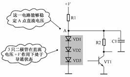
Fig. 9-40. A simple DC voltage regulator circuit, consisting of 3 conventional diodes
01 Network Analysis Ideas
It is difficult to analyze how a circuit works that has never been seen before, and even more difficult for beginners with incomplete basic knowledge.
The ideas behind analysis of this circuit are mainly explained as follows.
(1) It can be seen from diagram that 3 diodes are connected in series. According to characteristics of a series circuit, if 3 diodes are on, they will be on at same time, and if they are off, they will be off at same time.
(2) According to analysis of principle of determining whether diode is conductive or not, anode of diode is connected to a much higher voltage than cathode, whether it is DC or AC voltage, diode is in a state of conduction at this time. It can be seen from diagram that positive pole of VD1 is connected to a constant operating voltage +V in circuit through resistor R1, and negative pole of VD3 is grounded, due to which there are three diodes in series. From this analysis, you can find out that three diodes VD1, VD2 and VD3 turn on under influence of a constant operating voltage +V.
(3) It can also be seen from diagram that no AC signal voltage is added to three diodes, because between positive pole of VD1, that is, point A, to circuit and ground, as well as any AC signal voltage at point A. The voltage is shunted to ground.
02 Explanation of principle by which diodes can stabilize DC voltage
In circuit, three diodes turn on when DC operating voltage is forward biased, and effect on this circuit once turned on is to stabilize DC voltage at point A in circuit.
As we all know, interior of a diode is a PN junction structure. In addition to unidirectional conduction, a PN junction has many characteristics. One of them is that voltage drop across diode does not change much after diode is turned on. , For a commonly used silicon diode After word is turned on, voltage drop between positive pole and negative pole is 0.6V.
According to this characteristic of diodes, working principle of a simple DC voltage regulator circuit consisting of ordinary diodes can be easily analyzed. After turning on 3 diodes, voltage drop across tube of each diode is 0.6V, then DC voltage drop after connecting 3 diodes in series is 0.6×3=1.8V.
03 Fault detection method
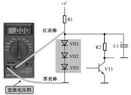
The most efficient way to detect three diodes in this circuit is to measure DC voltage across diodes, as shown in Figure 1. 9-41, which shows connection diagram for measurement. If result of measured DC voltage is about 1.8V, it means that three diodes are working normally; if result of measured DC voltage is 0 V, you need toWe can measure whether operating DC voltage + V is normal and whether resistor R1 is open. Three diodes are not involved, because three diodes. However, breakdown probability is small, if measured DC voltage is greater than 1.8V, check that one of three diodes faulty open circuit.
04 Circuit Failure Analysis
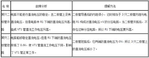
As shown in Table 9-40, failure analysis of this diode circuit
05 Circuit Analysis Details
The analysis details of above diode simple DC voltage regulator circuit are as follows.
(1) In circuit analysis, one-way conductance of a diode can be used to determine that diode is in a conduction state, but it does not explain specific effect of these diodes on circuit after conduction, so only one-way conduction is used Characteristics do not yet allow a correct analysis of principle scheme work.
(2) Among many characteristics of diodes, only characteristic that voltage drop across tube remains unchanged after conduction can most reasonably explain function of this circuit, therefore, based on it, it can be determined that this circuit is to stabilize A in DC point operating voltage circuits.
(3) If there are multiple components in circuit, you should try to identify main components that implement function of circuit, and then analyze around them. The analysis uses main characteristics of component to provide a reasonable explanation.
Diode Temperature Compensation Circuit and Troubleshooting
As we all know, after turning on PN junction, there is a voltage drop of about 0.6 V (meaning PN junction made of silicon material). characteristic: voltage drop after turning on PN junction basically does not change., but not unchanged, voltage drop at PN junction decreases slightly with increasing temperature, higher temperature, greater drop, of course, absolute value of voltage drop at PN junction is sufficient small - 0.6 V. With this function, you can form a temperature compensation circuit. As shown in fig. 9-42 is a temperature compensation circuit consisting of temperature characteristics of diode.
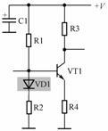
Figure 9-42 Diode temperature compensation circuit
It is not easy for beginners to understand that VT1 and other components in circuit constitute an amplifier, which is not suitable for analyzing principle of operation of this circuit. In circuit analysis, familiarity with circuit functions of VT1 block and other components has a positive value for analyzing principle of operation of VD1. Once function of a device circuit is understood, all circuit analysis can be done around it so that one can target it and get twice result with half effort.
01 Detailed circuit principle to be understood
Analysis of how this circuit works requires an understanding of following two principles of deep-level circuitry.
(1) VT1, etc. constitute amplifier circuit. The amplifier requires good stability. One of them is that triode quiescent current cannot change with temperature, i. base current of VT1 cannot change depending on temperature, otherwise stability will be poor. It is very important to understand temperature response of amplifier in order to understand how temperature compensation circuit made up of VD1 works.
(2) The VT1 triode has a poor temperature-related characteristic, that is, as temperature rises, base current of VT1 triode will increase, and higher temperature, greater base current, and vice versa. The stability of operation is not very good. It can be seen that poor temperature stability of amplifier is caused by temperature characteristics of triode.
02 Transistor bias circuit analysis
In circuit, when triode VT1 operates in an amplified state, a certain constant bias voltage must be applied to it, which is closed by a bias circuit. R1, VD1 and R2 in circuit form a dividing bias circuit to provide a constant operating voltage to base of triode VT1, and base voltage determines magnitude of base current VT1. If influence of temperature is not taken into account, and value of constant operating voltage +V is constant, then base constant voltage VT1 is stable, then base constant current of triode VT1 is constant, and triode can work stably.
When analyzing principle of operation of VD1 diode, one point needs to be clarified: VT1 is an NPN transistor, and its base DC voltage is high, so base current is large, otherwise it is small.
03 Analysis of VD1 diode temperature compensation circuit
According to position of VD1 diode in circuit, analysis of principle of its operation mainly explains following points:
(1) The positive pole of VD1 is connected to DC operating voltage +V through R1, and its negative pole is connected to ground wire through R2, so that VD1 is in a conductive state when DC current is applied. operating voltage +V. The key to understanding diode conductance is that voltage at positive pole is higher than voltage at negative pole.
(2) Explain how VD1 works incircuit using a voltage drop across lamp of 0.6 V after turning on diode is not possible, since DC operation required by base of VT1 can be achieved by adjusting resistance of resistors R1 and R2. The base voltage VT1 does not need to be regulated by turning on diode VD1 in series.
(3) The function of VD1 in circuit can be correctly explained using temperature characteristic of voltage drop across diode tube. If we assume that temperature rises, then according to characteristics of triode, base current VT1 will increase slightly. As temperature rises, voltage drop across VD1 diode tube will drop slightly, and voltage drop across VD1 tube will cause base voltage of VT1 to drop slightly, resulting in a drop in base current of VT1. From above analysis, it can be seen that after adding VD1 diode, initial temperature is increased to increase base current of VT1, and now VD1 circuit can reduce base current of VT1, which allows base current of triode VT1 to stabilize, so VD1 can play role of temperature compensation.
(4) The poor temperature stability of triode also manifests itself in process of lowering temperature. As temperature drops, base current of transistor VT1 will decrease, which is also a sign of poor temperature stability. After turning on VD1 diode, when temperature drops, voltage drop across its tube increases slightly, which increases constant operating voltage of VT1 base and, as a result, base current VT1 increases, which can also compensate for instability of VT1 triode when temperature drops.
04 Circuit Analysis Details
Details of schema analysis are described below.
(1) In circuit analysis, if a particular characteristic of a component can be used to reasonably explain its function in circuit, then circuit analysis is likely to be correct. For example, in circuit analysis above, only temperature characteristics of diode can be used to reasonably explain role of VD1 in circuit.
(2) The temperature compensation of temperature compensation circuit is bi-directional, that is, it can compensate for instability of circuit caused by temperature rise or fall.
(3) When analyzing working principle of temperature compensation circuit, it is necessary to assume that temperature will increase or decrease, and then analyze reaction process in circuit to obtain correct circuit feedback result. In actual circuit analysis, it is only necessary to set temperature rise to analyze circuit compensation, and there is no need to analyze circuit compensation when temperature drops, because circuit analysis ideas and temperature drop processes are similar, but changes in each step of circuit analysis are opposite.
(4) In above circuit analysis, temperature characteristics of PN junction (emitter junction) between base of VT1 and emitter are similar to those of VD1, since they are bothare PN junction structures, so temperature compensation results are relatively good.
(5) The diode VD1 in above circuit does not have a stabilizing effect on +V DC operating voltage fluctuation, so it cannot compensate for DC operating current instability at base of VT1 lamp caused by +V DC operating voltage fluctuation.
05 Fault detection method and circuit fault analysis
The method for detecting faulty diode VD1 in this circuit is relatively simple. You can use multimeter's ohmic gear to measure forward and reverse resistance of VD1 on road.
When VD1 circuit is broken, constant bias voltage based on triode VT1 increases greatly, which leads to transition of VT1 lamp to a saturation state. burned out VT1. In event of a breakdown of VD1, constant bias voltage of VT1 lamp base will drop by 0.6V, constant operating current of VT1 triode will decrease, and amplifying ability of VT1 lamp will decrease or enter a critical value. cutoff state.
Diode driving circuit and troubleshooting
After turning on diode, its forward resistance changes slightly with current change: greater forward current, lower forward resistance, and vice versa.
Using characteristics between forward current and forward resistance of a diode, some automatic control circuits can be formed. As shown in fig. 9-43, this is an automatic control circuit composed of diodes, also known as an ALC circuit (automatic level control circuit), which is often used in recording circuit of magnetic recording equipment (such as a deck).
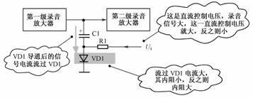
Figure 9-43 Diode automatic control circuit
01 Description of knowledge to prepare for circuit analysis
The one-way conduction characteristic of a diode only shows that forward resistance is small and reverse resistance is large, but does not explain specific characteristics of diode after it is turned on.
After a diode is driven in forward direction, its forward resistance is also related to forward current flowing through diode. Although forward resistance of diode after forward conduction is relatively small (compared to reverse resistance), as forward current increases, forward resistance of diode after forward conduction will decrease even more, i.e. greater forward current, greater forward resistance, lower resistance , and vice versa.
Ignorance of function of circuit is bad for principle of operation of circuit. Against background of understanding function of a circuit, you can analyze how circuit works or function of a particular component in circuit.
The AGC circuit is located on recording board of tape recorder and deck. When recording, it is necessary to control size and amplitude of recorded signal. Understanding following specific control requirements is useful for analyzing VD1 diode of machine. control circuit.
(1) When amplitude of recording signal is small, amplitude of recording signal is not controlled.
(2) When amplitude of recording signal is large enough, amplitude of recording signal is controlled, that is, amplitude of signal is attenuated. The circuit that controls amplitude of recording signal is called ALC circuit.
(3) After ALC circuit enters control state, more write signal is required, greater attenuation of signal.
It can be seen from above description that circuit analysis requires you to have a relatively comprehensive knowledge that must be accumulated through continuous learning.
02 Explaining ideas behind circuit analysis
Analysis of working principle of this circuit mainly explains following points:
(1) If there is no VD1 tap, all recording signals output from first stage recording amplifier are added to second stage recording amplifier. However, with VD1 branch, recording signal coming out of recording amplifier of first stage can enter ground terminal through C1 and conduction of VD1, forming a shunt attenuation of recording signal.
(2) The second key of circuit analysis is specific situation of shunt attenuation of VD1 branch to ground of output signal of recording amplifier of first stage. Obviously, capacitor C1 in branch circuit is a large capacitor (the polarity is marked in diagram with symbol C1, which indicates that C1 is an electrolytic capacitor, and capacitance of electrolytic capacitor is large), so C1 is path to write signal, indicating that this VD1 is in one branch is a key component for shunting and attenuating recording signal.
(3) ANDFrom analysis of shunt branch circuit, one point should be understood: if signal output from recording amplifier of first stage is more shunted from VD1 branch, then recording signal entering second recording stage of amplifier will be small, but on contrary large.
(4) VD1 has two situations of conduction and cutoff: when VD1 is off, it has no shunt effect on write signal, and when it is on, it shunts write signal.
(5) A resistor R1 is connected to positive pole of VD1, which supplies a control voltage to VD1, obviously, this voltage controls VD1 on or off. Therefore, voltage sent by R1 is key to analyzing VD1 on and off.
The biggest difficulty in analyzing this circuit is that after turning on VD1, relationship between direct resistance and conduction current of diode is used to analyze circuit, that is, greater forward current of diode, greater forward current. The lower resistance, greater current flowing through VD1, less resistance between its positive and negative electrodes, and vice versa.
03
Description of common control circuit analysis methods
Control circuit analysis is usually divided into several situations, for example, control signal is divided into several situations, such as large, medium and small. With regard to this circuit, control of diode VD1 by control voltage Ui is divided into following situations.
(1) When there is no recording signal in circuit, DC control voltage Ui is 0, diode VD1 is off, and VD1 does not affect operation of circuit, and all signals output from first stage recording amplifier can be added to recording amplifier of second stage .
(2) When write signal in circuit is small, DC control voltage Ui is small and does not exceed conduction voltage of diode VD1, so it is not enough to make diode VD1 conduct. , diode VD1 - recording amplifier of first stage. The output signal also has no shunting effect.
(3) When write signal in circuit is relatively large, constant control voltage Ui is relatively large, and diode VD1 is turned on, internal resistance is smaller.
(4) After turning on VD1, internal resistance of VD1 drops, and part of recording signal output by recording amplifier of first stage is shunted to ground terminal through capacitor C1 and switched on diode VD1. , and deeper inclusion of VD1, lower its internal resistance, greater shunt flux to ground of output signal of recording amplifier of first stage and automatic level control is implemented.
(5) The conduction degree of VD1 diode is controlled by DC control voltage Ui, and DC control voltage Ui changes with size of write signal in circuit, so change in internal resistance of VD1 is actually controlled by size of write signal.
04 Update methodFault detection and circuit fault analysis
The best way to find a faulty diode in this circuit is to replace it, because poor diode performance will also affect driving effect of circuit.
When VD1 diode is open, control function does not work. At this time, when recording a large signal, sound will fluctuate and be distorted. When recording signal is small, recording may be normal.
When diode VD1 is broken, control function does not work. At this time, recorded sound is very weak, since recording signal is shunted to ground by broken diode VD1.
Diode Clamp Schematic and Troubleshooting
The most basic operating state of a diode is on and off, and this characteristic can be used to form a limiter circuit. The so-called limiting circuit is designed to limit signal amplitude at a certain point in circuit, so that when signal amplitude is large to a certain extent, signal amplitude cannot increase again. When signal amplitude does not reach limited amplitude, limiting circuit does not work. The circuit with this function is called clipping circuit, and a circuit that uses a diode to perform this function is called a diode clipping circuit.
As shown in fig. 9-44 is a diode clamp circuit. In circuit, A1 is an integrated circuit (common element), VT1 and VT2 are triodes (common element), R1 and R2 are resistors, and VD1~VD6 are diodes.
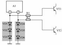
Figure 9-44 Diode suppressor circuit
01 Network Analysis Ideas
The idea of analyzing function of VD1 and VD2 in circuit basically explains following points:
(1) It can be seen from diagram that circuit structure of two groups of diodes VD1, VD2, VD3 and VD4, VD5, VD6 is same, and functions of these two groups of diodes in this circuit are same, so just analyze working principle of one set of diode circuits.
(2) Pin ① of A1 is connected to base of triode VT1 through resistor R1. Obviously, R1 is a signal transfer resistor. There is no current between terminal and base of triode VT1. From this circuit structure, it can be judged that terminal ① of integrated circuit A1 is an output signal terminal, and it outputs a composite DC/AC signal. The purpose of determining that terminal ① of integrated circuit A1 is a signal output terminal is to judge specific function of diode VD1 in circuit.
(3) The DC voltage output at ① pin of integrated circuit is obviously not very high, not so high that external diode is in conduction. The reason is that if DC output voltage at IC pin ① If circuit A1 is high enough, VD1, VD2 and VD3 turn on, and internal resistance after they turn on is very small, which shunts AC output signal from pin ① of A1 integrated circuit to ground and attenuates signal. Obviously, there is no need to perform signal processing in this circuit .Such attenuation, so conclusion derived from analysis from this point of view: output DC voltage at pin ① of integrated circuit A1 will not be high enough to turn on VD1, VD2 and VD3.
(4) The output from terminal ① of integrated circuit A1 is a superimposed DC and AC signal, through resistor R1 and base of transistor VT1, VT1 is an NPN transistor, if amplitude of positive half appears AC signal added to base of VT1 . A very large phenomenon will cause base voltage of VT1 to be very large, and there will be a danger of burning out VT1. With a large amplitude of negative half-cycle of alternating signal added to base of VT1, there is no effect on burnout of VT1, since signal of negative polarity on base of VT1 reduces current of base of VT1.
(5) Based on above circuit analysis ideas, it can be tentatively judged that VD1, VD2, and VD3 in circuit are clamper protection diode circuits to prevent positive half-wave amplitude of AC signal output from ① pin of A1 integrated circuit due to fact that it is too large and burns out VT1.
Based on above ideas, perform further analysis of diode circuits VD1, VD2, VD3. If analysis is logical, it can show that above network analysis ideas inerny.
02 Diode clipping circuit
There is a way to analyze operation of various limiting circuits, and signal amplitude is divided into two situations:
(1) The operating state of circuit when signal amplitude is relatively small, that is, signal amplitude is not large enough to operate limiter circuit, and limiter circuit is not working at that time.
(2) The working state of circuit when signal amplitude is relatively large, that is, signal amplitude is large enough to allow amplitude limiting circuit to work. At this time, limiting circuit works to limit signal amplitude.
Using waveform drawing method to analyze how a circuit works is sometimes very useful, especially when analyzing a limiter circuit. integrated circuit A1 in circuit.
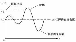
Figure 9-45. Schematic diagram of waveform at pin ① of integrated circuit A1
In figure, U1 represents DC voltage at output signal of pin ① of integrated circuit A1, and AC voltage at output signal of pin ① depends on this DC voltage. U2 - voltage limit value.
Combining above waveform to analyze clamping circuit of diode, when AC voltage in output signal of ① pin of integrated circuit A1 is relatively small, positive half-cycle of AC signal plus DC output voltage of U1 does not reach VD1, VD2 and VD3 Degree of conduction , so all diodes are off, which does not affect AC signal output by pin ①, and AC signal is added to VT1 through R1.
Assume that amplitude of positive half-cycle of AC signal output from ① terminal of integrated circuit A1 is very large for a certain period, as shown in waveform in Fig. 8-12 because amplitude of positive half-cycle of AC signal plus DC voltage has exceeded diode. The forward conduction voltage values VD1, VD2 and VD3, if conduction voltage of each diode is 0.7 V, then conduction voltage of three diodes is 2.1 V. terminal ① of integrated circuit A1 is 2.1 V, excess part of positive half-cycle of AC signal is removed (limited), and excess signal is actually reset to integrated circuit, to resistor in circuit at terminal ① A1 (not shown in figure).
When amplitude of DC and AC output signals at ① terminal of integrated circuit A1 is less than 2.1V, this voltage cannot make 3 diodes conduct, so that 3 diodes switch from conduction to cutoff again, which does not affect effect signal limits.
03 Circuit Analysis Details
Specific analysis details for this circuit are described below.
(1) Negative half-cycle large amplitude signal output from A1 IC pin ① will not cause VT1 overcurrent because negative half-cycle signal will only reduce base voltage and base current of NPN transistor, so there is no need to add a negative half-cycle limiter circuit .
(2) The one-way clipping circuit shown above can clip only positive half cycle or negative half cycle of signal, but not clip other half cycle of signal. The other is a two-way clipping circuit that can simultaneously clip positive and negative half-cycle signals.
(3) There are many reasons for abnormal increase in signal amplitude, such as random factors (such as fluctuations in supply voltage) cause a strong increase in signal amplitude at a certain moment, and large-scale interference pulses from outside enter circuit. It is also a common cause of an abnormal increase in signal at a certain moment.
(4) After turning on three diodes VD1, VD2 and VD3, sum of DC and AC voltages at pin ① of integrated circuit A1 is 2.1V, and this voltage is added to base of VT1 through resistor R1, which is also maximum base voltage of VT1 , base current at this time is also maximum base current VT1.
(5) Since outer circuits of terminal ① and terminal ② of integrated circuit A1 are same, limiting protection circuit in outer circuit works on same principle, and only one circuit needs to be analyzed when analyzing circuit. .
(6) According to characteristics of series circuit, current in series circuit is same everywhere, so we can know that three series diodes VD1, VD2 and VD3 conduct current at same time, otherwise they will break. turns off at same time and there will never be a series circuit. A certain diode is on and some diodes are off.
04 Fault detection method and circuit fault analysis
In order to detect failure of diode in this circuit, ohmic gear of multimeter is mainly used to measure its forward and reverse resistance on road, because diode in this circuit does not work in DC circuit, so DC current at both ends of diode is measured Pressure drop method does not fit.
The diodes in this circuit are less likely to fail because they operate in weak signal conditions. If diode in circuit is open, circuit will not have a limiting effect, which will affect normal operation of subsequent stage circuit.
Diode Switch Schematic and Troubleshooting
A switch circuit is a commonly used functional circuit, such as a switch in a lighting circuit in a house, a power switch in various household appliances, etc.
There are two types of switches in switching circuits:
(1) Mechanical switches using mechanical switches as switching circuit components.
(2) Electronic switches, so-called electronic switches, do not use mechanical switching elements, but use devices such as diodes and triodes to form switching circuits.
01 Description of diode switching characteristics
Switching diodes are same as ordinary diodes, and they also have a PN junction structure, difference is that switching performance of this diode should be better.
When a forward voltage is applied to switching diode, diode is in conductive state, which is equivalent to on state of switch; when reverse voltage is applied to switching diode, diode is in off state, which is equivalent to switch off state. VCThe on and off states of diode complete on and off functions.
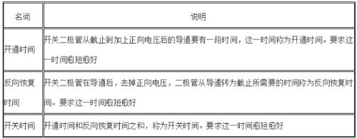
Switching diodes use this characteristic, and due to manufacturing process, switching characteristics are better, that is, switching speed is faster, PN junction junction capacitance is smaller, internal turn-on resistance is smaller. , and resistance in off state is large. . Table 9-41 shows concept of switching times.
Table 6.19 Description of switching time concept
02 Typical operating principle of a diode switching circuit
Switching electronic circuits made up of diodes come in a variety of forms, as shown in fig. 9-46 for a typical diode switching circuit.
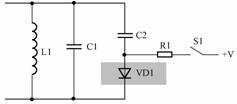
Figure 9-46 Diode switch circuit
Watching this circuit, you can become familiar with following aspects that will make it easier to understand how circuit works:
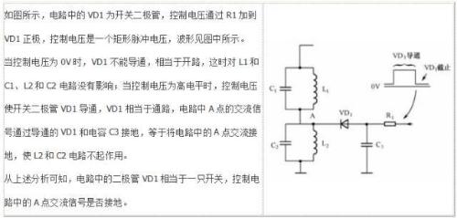
(1) Understanding function of this device diagram is first step. From circuit shown in Figure 8-14, it can be seen that inductor L1 and capacitor C1 are connected in parallel, which is obviously LC parallel resonant circuit, which is main function of this unit circuit. After clarifying this point, we can know that other components in circuit should be an auxiliary component around this main function, an extension or addition to main function of circuit, etc. This way of thinking can easily analyze function of components in circuit.
(2) C2 and VD1 form a series circuit, and then connected in parallel with C1. From this circuit structure, we can conclude: function of branch of C2 and VD1 is to change parallel connection with capacitor C1 through this branch. The reason for this judgment in that total capacitance of branches C2 and VD1 is connected in parallel with C1, and oscillation frequency of LC-parallel resonant circuit formed with L1 is changed. So this is a circuit that changes frequency of an LC parallel resonant circuit.
The following points are explained by analyzing diode electronic switch circuit:
(1) In a circuit, C2 and VD1 are connected in series. According to characteristics of a series circuit, C2 and VD1 are either connected to circuit at same time or disconnected at same time. If only C2 needs to be connected in parallel with C1, C2 can be connected directly in parallel with C1, but VD1 diode is in series, indicating that VD1 controls connection and disconnection of C2.
(2) According to conductance and cutoff characteristics of diode, VD1 is turned on when C2 is required to be connected to circuit, and VD1 is turned off when C2 is not required to be connected to circuit. This diode working mode is called switching mode, such a circuit is called a diode switching circuit.
(3) The conductance and cutoff of diode must be controlled by voltage. In circuit, anode VD1 is connected to +V constant voltage terminal through resistor R1 and switch S1. This voltage is control voltage of diode.
(4) Switch S1 in circuit is used to control whether operating voltage +V is connected to circuit. From circuit of switch S1, it is easier to confirm that diode VD1 is operating in switch state, since turning S1 on and off controls conduction and cutoff of diode. As shown in Table 9-42, this is a description of working principle of diode electronic switch circuit.
Table 9-42 Explanation of working principle of diode electronic switch circuit
In above two states, due to different capacitances in LC parallel resonant circuit, in one case only C1, and in other case C1 and C2 are connected in parallel, and resonant frequency of parallel LC resonant circuit is different under condition of different capacitances. Therefore, real function of VD1 in circuit is to control resonant frequency of LC-parallel resonant circuit.
The following two points are explained in detail when analyzing diode electronic switch circuit:
(1) When there is a switch in circuit, circuit analysis takes two cases of switching on and off of switch as examples to analyze working state of circuit, respectively. So when a switch appears in a circuit, it can provide insights for circuit analysis.
(2) The signal in LC parallel resonant circuit is added to positive pole of VD1-C2, but because amplitude of signal in resonant circuit is relatively small, amplitude of positive half-wave signal added to positive pole of VD1 is very small, which does not ensure conduction of VD1.
03 Fault detection method and circuit fault analysis
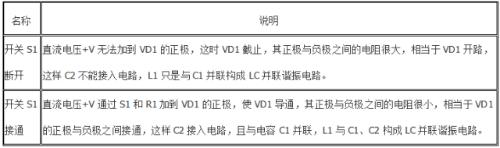
As shown in Figure 9-47, this is circuit diagram for connecting switching diode in detection circuit. When switch is turned on, measure DC voltage drop across diode VD1. It should be 0.6V. If it is much lower than this voltage value, it means that VD1 is shorted. A little less than this voltage value indicates that VD1 has an open circuit. In addition, if there is no obvious short circuit or open circuit VD1, you can measure its direct resistance with a multimeter, it should be small, otherwise it’s not good if the direct resistance is too high.
Figure 9-47 Wiring diagram for switching diodes in detection circuit
If switching diode in this circuit is open or shorted, oscillation frequency cannot be adjusted. With switching diode open, capacitor C2 cannot be connected to circuit, and oscillation frequency increases at this time; when switching diode is short-circuited, capacitor C2 is always connected to circuit, and oscillation frequency decreases at this time.
04 Analysis of how such circuits work
Diode detection circuit and troubleshooting
As shown in fig. 9-48 is diode detection circuit. VD1 in circuit is a detection diode, C1 is a high-frequency filter capacitor, R1 is load resistance of the detection circuit, C2 is a coupling capacitor.
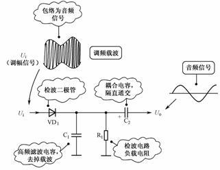
Figure 9-48 Diode detection circuit
01 Knowledge of preparing for circuit analysis
As we all know, there are two types of radios: AM radio and FM radio. AM signal is a signal that is processed and amplified in AM radio. See schematic diagram of AM signal waveform in figure. The following points are explained mainly for this signal waveform:
(1) What comes from AM radio antenna is an AM signal.
(2) The middle part of signal is high frequency carrier signal, and its high and low ends are envelope of AM signal, and its envelope is desired audio signal.
(3) The upper envelope signal and lower envelope signal are symmetrical, but phase of signal is opposite. Finally, radio only needs upper envelope signal, lower envelope signal is not used, and high-frequency carrier signal in middle is not needed.
02 Description of function of each component in circuit
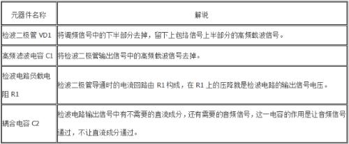
As shown in Table 9-43, this is an explanation of functions of components.
Table 9-43 Description of component functions
03 Analysis of how detection circuit works
The detection circuit mainly consists of detector diode VD1.
In detection circuit, an AM signal is added to anode of detector diode. At this time, working principle of detector diode is basically same as that of rectifier diode in rectification circuit. The amplitude of signal is used to conduct detection diode, as shown in fig. 9. In fig. 49 shows a diagram of an extended AM signal.
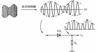
Figure 9-49. Schematic diagram of extension along time axis of AM signal
You can see from expanded AM waveform that this is an AC signal, but amplitude of signal varies. This signal is applied to anode of detector diode, positive half-cycle signal makes diode conduct, and negative half-cycle signal turns off diode, which is equivalent to rectification circuit, and envelope of positive half-cycle signal is obtained at load resistance R1 of detector diode, that is, signal. For part indicated by dotted line, see output waveform of detection circuit in figure (output waveform with no high-pass filter). added capacitor).
The output of detection circuit consists of three signal components: an audio signal, a DC component, and a high-frequency carrier signal. It is necessary to carry out a detailed analysis of circuit according to three signal states. Of these three signals, most important is analysis and understanding of how audio signal processing circuits work.
(1) The desired audio signal is output signal envelope as shown in Figure 9-50. This audio signal is passed through output capacitor C2 of detector circuit and sent to next circuit for further processing.
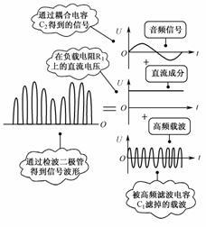
Figure 9-50 Schematic diagram of detector circuit output waveform
(2) The average value of output of detection circuit is DC. Its size is average amplitude of output of detection circuit. The output of detection circuit has a large amplitude and a large average value is large, and vice versa. This DC component is used in radio circuits to control gain (also called gain) of a type called an IF amplifier, known as AGC (Automatic Gain Control) voltage. The AGC voltage is isolated by a decoupling capacitor at output of detection circuit and cannot be added to post-amplifier circuit along with audio signal, but is added exclusively to AGC circuit.
(3) There is also a high-frequency carrier signal in output of detection circuit. This signal is useless. It is filtered to ground terminal through high-pass filter capacitor C1 connected to output terminal of detection circuit.
From detection circuit, it can be seen that high-pass filter capacitor C1 is connected between output end of detection circuit and ground wire. Since three signals at output of detection circuit have different frequencies, and capacitance of high-pass filter capacitor C1 is very small, so C1 processes three signals according to in different ways.
(1) For DC voltage, DC blocking characteristics of capacitor make C1 open, so DC output of detector circuit cannot be shunted to ground by C1.
(2) For an audio signal, because capacitance of high-pass filter capacitor C1 is very small, it has a large capacitance to audio signal, which is equivalent to an open circuit, so audio signal cannot be bypassed to ground by C1.
(3) For a high-frequency carrier signal, its frequency is very high and capacitance C1 is very small, and it is in a passing state. Therefore, only high-frequency carrier signal at output of detection circuit is grounded by capacitor C1. It acts as a high pass filter.
As shown in fig. 9-51, there are three kinds of signal current circuits after detector diode is turned on. A terminating resistor forms a DC loop, and a coupling capacitor outputs an audible signal.
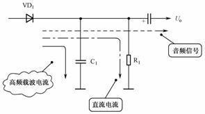
Figure 9-51 Schematic diagram of three signal current loops after switching on detector diode
04 Fault detection method and circuit fault analysis
Detection diode cannot be detected by DC voltage measurement, because this type of diode does not work at DC voltage, so forward and reverse resistance measurement method should be used to judge quality of detection diode.
When detection diode is open or has a short circuit, detection task cannot be completed, so radio circuit will have a silent radio fault.
05 Analysis of working principle of a practical voltage doubler detection circuit
As shown in Figure 9-52, this is a practical dual voltage detection circuit. C2, VD1 and VD2 in circuit form a dual voltage detection circuit, which is used to convert AM signal to audio signal in radio station. scheme. C3 in circuit is filter capacitor after detection. The audio signal received by this dual voltage detection circuit is added to audio amplifier tube through decoupling capacitor C5.
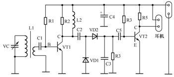
Figure 9-52. Practical Circuit for Doubling Voltage Detection
Diode Protection Circuit and Relay Control Troubleshooting
The relay has a coil structure inside, so when it is turned off, it will generate reverse electromotive force with a large voltage, which will cause relay control transistor to fail. For this reason, a diode protection circuit must be installed in relay drive circuit to protect relay drive tube.
As shown in Figure 9-53, this is diode protection circuit in relay control circuit. J1 in circuit is relay, VD1 is protective diode of VT1 drive tube, and R1 and C1 are spark arrester. diagram of internal switching contacts of the relay.
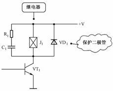
Figure 9-53 Diode protection circuit
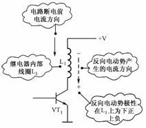
Figure 9-54 Equivalent circuit
01 Analysis of how circuit works
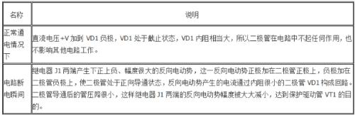
There is a group of coils inside relay, as shown in Figure 9-54, which is an equivalent circuit. Before relay is deactivated, direction of current flowing through relay coil L1 is from top to bottom. After power is turned off, coil creates a reverse electromotive force. Block this change in current, that is, generate a current flowing from top to bottom, as shown by dotted line in figure. According to method of distinguishing back EMF at both ends of coil described above, it can be known that polarity of back EMF on coil L1 is positive at bottom and negative at top, as shown in Fig. figure. As shown in Table 9-44, this is a description of how protection diode works in this circuit.
Table 9-44 Protection Diode Description
02 Fault detection method and circuit fault analysis
For protection diode in this circuit, method of measuring DC voltage drop across diode cannot be used to evaluate fault detection, nor can method of measuring forward and reverse resistance of diode on road be used. because two ends of diode are connected in parallel. The relay coil has very little DC resistance, so diode quality cannot be judged by voltage drop. An alternative to inspection should be used.
When protection diode is open, it does not have much effect on working state of relay circuit, but there is no protective effect, and it is very likely that drive tube will fail; when protection diode is short-circuited, it is equivalent to short circuiting relay coil, then there is no current in relay coil and relay cannot work.
Related
- (Detailed long text) 7 ways to use diodes that engineers need to master
- "English abbreviations" that equipment engineers need to know
- A Few Design Tips PCB Engineers Need to Know
- How to effectively use an oscilloscope? Even senior engineers overlook these details...
- Do you know four magical ways to use a digital multimeter?
- Welding knowledge and skills that electronics professionals need to understand
- must read! Electronics Engineers Must Master 7 Common Interfaces in Circuits
- 7 things you need to know about high-speed linking and routing
- Why are circuit boards mostly green? See what these 20+ engineers have to say
- What you need to know about semiconductor chips
Hot Posts
 How to distinguish induction from leakage, we will teach you three tricks! Ordinary people can also learn super practical
- What is drowning in gold? Why Shen Jin?
- This is a metaphor for EMI/EMS/EMC that can be understood at a glance.
- How many types of pads have you seen in PCB design?
- Summary of Common PCB Repair Techniques
- What is three anti-paint? How to use it correctly?
- Knowing these rules, you will not get confused looking at circuit diagram.
- How to make anti-interference PCB design?
- Can diodes do this?