Location:Home Page > Archive Archive
Detailed analysis of the "various protection schemes" of a switching power supply
2023-04-09【Archive】
Input undervoltage protection circuit 1
01 Overview
This circuit refers to undervoltage input circuit. When input voltage is lower than protection voltage, control chip's Vcc power supply is turned off to turn off output.
02 Circuit composition (principle diagram)
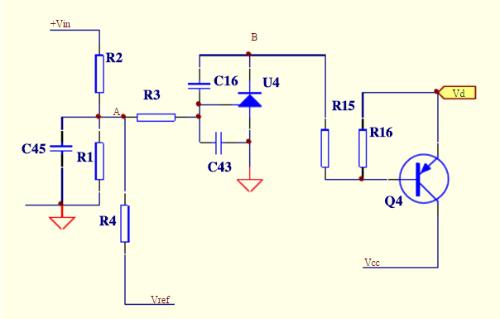
03 Operation principle analysis
When power supply input voltage is higher than undervoltage protection setting, voltage at point A is higher than Vref U4, U4 turns on, voltage at point B is low, Q4 turns on, and power supply Vcc is normal; when input voltage is low At protection voltage, voltage at point A is lower than Vref U4, U4 is turned off, voltage at point B is high, and Q4 is turned off, so Vcc has no voltage, and Vref is also low at this time. When input voltage gradually increases , voltage at point A also increases gradually, and when it is higher than Vref U4, module works normally again. R4 can set hysteresis of undervoltage protection point.
Advantages and disadvantages of Schemes 04
Benefits:Simple circuit, precise point of protection
Cons: higher cost.
Notes for applications 05
When using, pay attention to values of R1 and R2, sometimes two resistors need to be connected in parallel to get required protection point. It is also necessary to pay attention to temperature coefficient of R1 and R2, otherwise undervoltage protection point will be very different at high and low temperature.
Input undervoltage protection circuit 2
01 Overview
Input undervoltage protection circuit. When input voltage is lower than set minimum voltage value, output turns off; when input voltage rises to set recovery value, output will automatically return to normal.
02 Circuit composition (principle diagram)
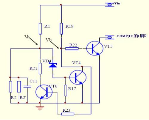
03 Operation principle analysis
When input voltage is within normal operating range, Va is greater than adjustable value of VD4, VT4 is turned on, Vb is at potential 0, and VT5 is turned off, at this time protection circuit does not work. ; when input voltage is below set value of minimum voltage. When Va is less than adjustable value of VD4, VT4 turns off, Vb is high potential, VT5 turns on, and COMP (pin 1 of microcircuit) is pulled up to 0, and microcircuit turns off output, thereby realizing undervoltage protection function. R21, VT6 and R23 form a hysteresis circuit for undervoltage shutdown and recovery. When minimum voltage is turned off, VT6 is turned on, and R21 and R2 are connected in parallel, 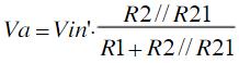 ; When restoring, VT6 is cut off,
 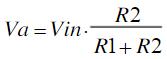 , hysteresis voltage (Vin’-Vin).
Advantages and disadvantages of Schemes 04
Benefits: The shape of circuit is simple and cost is low.
Disadvantages: Due to difference in voltage regulation value of VD4 voltage regulator tube between batches, undervoltage protection point fluctuates up and down, and corresponding parameters need to be adjusted frequently during mass production.
Notes for applications 05
VD4, choose Zener tube with best temperature coefficient. For components that require debugging, such as R2, several parallel connections should be considered to facilitate debugging.
Input 1 surge protection
01 Overview
Output overvoltage protection circuit. This circuit will clamp output voltage at a set value when an external voltage is applied to output terminal that exceeds normal output voltage range, or when circuit itself fails (open loop or whatever) causing output voltage to exceed adjustable value. value.
02 Circuit composition (principle diagram)
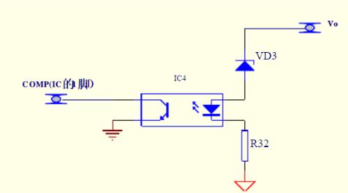
03 Operation principle analysis
When output is over-voltage, when voltage added to VD3 exceeds its adjustable value, VD3 turns on, output voltage is fixed, and feedback to primary side is carried out through IC4.
Advantages and disadvantages of Schemes 04
Benefits: The shape of circuit is simple and cost is low.
Disadvantages: Due to difference in voltage regulation value of VD3 voltage regulator tube between batches, overvoltage limiting point fluctuates up and down, and related parameters need to be adjusted frequently during mass testing. production.
Notes for applications 05
VD3, choose Zener tube with best temperature coefficient. For components requiring debugging, such as R32, several parallel connections should be considered to facilitate debugging.
When surge protection circuit is working, circuit is in an abnormal working state. For a circuit with function of adjusting output voltage up and down, overvoltage protection point must be greater than maximum value of output voltage.
Input 2 surge protection
01 Overview
Output overvoltage protection circuit. This circuit stabilizes output voltage at a set value when a voltage exceeding normal output voltage range is applied to output terminal, or when circuit itself fails (open loop or otherwise), causing output voltage to be higher than normal.
02 Circuit composition (principle diagram)
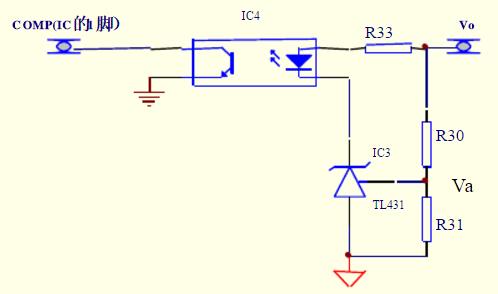
03 Operation principle analysis
When there is an overvoltage at output, Va>Vref, IC3 turns on, and feedback to primary side through IC4, output voltage is stable at set overvoltage protection value.
Advantages and disadvantages of Schemes 04
Benefits: The output overvoltage protection value can be set precisely.
Disadvantages. Compared with voltage regulator clamp method, cost is slightly higher.
Notes for applications 05
When surge protection circuit is working, circuit is in an abnormal working state. For a circuit with function of adjusting output voltage up and down, overvoltage protection point must be greater than maximum value of output voltage.
Self-locking surge protection control circuit
01 Overview
In a power system, when feedback loop fails, output voltage is out of control and voltage is out of specified range. At this time, excessive output voltage can damage downstream electrical equipment. To solve this problem, an overvoltage protection circuit is usually added to power supply. Generally, there are three surge protection methods.
A. Limit Type: When feedback fails, output voltage will be fixed at a fixed value by overvoltage limiting circuit.
B. Intermittent protection type: when feedback fails, output voltage is restarted back and forth through protection circuit, and highest point of output voltage is overvoltage protection point.
C. Self-locking type: when output voltage reaches overvoltage protection point, circuit will actuate and turn off PWM so that module has no output. After troubleshooting, restart power output to ensure normal power supply. The following circuit is a self-locking control circuit.
02 Circuit composition (principle diagram)
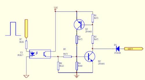
03 Operation principle analysis
The figure above shows an isolated self-locking control circuit. When overvoltage protection signal CONTROL end goes high, triode in U1 turns on and VCC is power supply end of entire circuit. Vcc supplies base current to Q2 through R5, Q1 turns on and saturates, SHUT terminal is pulled low by Q2, and PWM turns off power supply with no output. Q2 also controls conductance of Q1. When Q2 is on, Q1's base current goes to ground through R2, Q1 turns on, and base current is applied to Q2 through R3 to keep Q2 conductive. Q1 and R1, R2, R3 form positive feedback loop Q2.
Advantages and disadvantages of Schemes 04
Benefits: Efficient self-locking protection, whole circuit is equivalent to a silicon driven rectifier.
Cons: The whole circuit requires a fixed Vcc. If there is no power at PWM power terminal, it is also necessary to ensure that VCC voltage in above figure is present.
Notes for applications 05
1. This circuit must have a continuous power supply and self-locking to be effective.
2. This circuit cannot be used in an unattended power system.
Overheat protection circuit
01 Overview
This circuit is an overtemperature protection circuit, but when temperature is higher than set protection point, output of module is turned off, and module automatically turns on when temperature is restored.
02 Circuit composition (principle diagram)
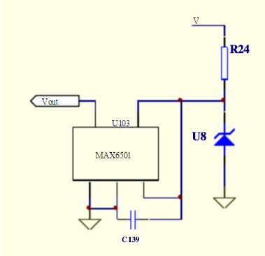
03 Operation principle analysis
The Zener tube supplies 5V to U103MAX6501. At normal temperature, five pins of U103 output a high level. When temperature exceeds protection point, five pins of U103 output low. five pins of U103 output a high level.
Advantages and disadvantages of Schemes 04
Benefits: simple circuit and high accuracy.
Cons: higher cost.
Notes for applications 05
1. When pin 3 of MAX6501 is connected to pin 1, hysteresis temperature is 10°C, and when pin 3 is connected to ground, hysteresis temperature is 2°C.
2. The supply voltage of MAX6501 cannot exceed 7V or it will be damaged.
3. The MAX6501 should be located near hottest part.
Thermistor thermal protection circuit
01 Overview
This circuit uses a thermistor to sense temperature of substrate. The resistance of thermistor varies with temperature of substrate. The change in resistance of thermistor causes input voltage of op-amp to change, thereby realizing op-amp flip to drive output of PWM chip, and then close module.
02 Circuit composition (principle diagram)
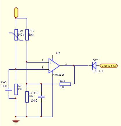
03 Operation principle analysis
Thermistor R99 is an NTC thermistor. At room temperature, R99=100k, divided voltage of R99 and R94 is 0.45V, which is negative input of op-amp U2, which is much lower than positive input of op-amp 2 .5V (R23 and R97), so output of op-amp is high, which does not affect end of SS LM5025, and module works normally.
As substrate temperature increases, R99 resistance decreases. When it decreases to a certain value, negative input of op-amp is larger than positive input, and op-amp outputs a low level, which pulls LM5025 SS low. So module output is turned off, temperature protection point can be adjusted by adjusting values of resistances R94, R23 and R97.
After module turns off output (overtemperature protection), temperature of substrate will drop, resistance R99 will increase, and negative input of op-amp will decrease. turn normally, resistor R98 is inserted. After a low level, R98 is equivalent to being connected in parallel with R97, lowering op-amp reference and increasing voltage gap between positive and negative inputs of op-amp, thereby realizing thermal hysteresis. For example, at a substrate temperature of 90°C it is protected, and at 80°C it is on.
04 Calculation and analysis of key parameters
1. Op-amp positive input voltage: VR97=Vref2=5/(1+R23/R97)=5/(1+10/10)=2.5V
2. Op Amp Negative Input Voltage
VR94+0.007=VR97=5*R94/(R99+R94)+0.007,
3. Get thermistor resistance value for temperature protection: R99(t)=(Vref*R24/(Vref*R97/(R23+R97)-0.007))-R94
4. The tolerance calculation is shown in table below:
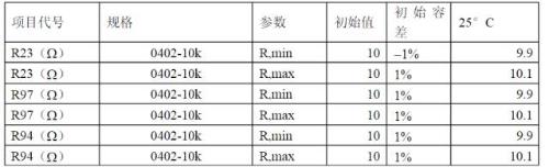
5. R99 value for overtemperature protection
6. R99-SDNT2012X104J4250HT(F) is an NTC thermistor, 100k at 25°C, with a resistance value of about 10k in overheat protection (see table above), design temperature: /p>
Rt=R*e(B(1/T1-1/T2)) T1=1/(ln(Rt/R)/B+1/T2))
T2: normal temperature 25°C, T2=273.15+25=298.15 in above formula, B: 4250±3%, R: resistance value at 25°C, 100k, T1 calculated value also after adding 273.15 So t1=T1-273.15 in following table corresponds to degrees Celsius. Rt: resistance value after temperature change, 10k, 9.704k, 10.304k, see table above.
7. Hysteresis
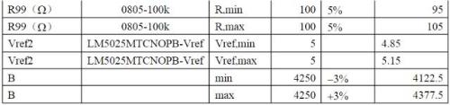
After output of op-amp goes low, resistor R98 (51 kΩ) is connected to R97 to lower reference voltage, and new reference voltage is Vref1=Vref*(R98//R97)/(R23+R98/ / R97)=2.28 When V reaches 2.44V, resistance value of R99 R99=Vref*R94/Vref1-R94=11.9KΩ When R99 reaches 10.49KΩ, temperature is calculated according to table
Temperature hysteresis=82.6-77.3=5.3℃
Advantages and disadvantages of Scheme 05
Benefits: Temperature protection point and temperature hysteresis are easily adjustable
Disadvantages: Poor temperature accuracy
The circuit is slightly more complicated than using a temperature switch. The temperature protection reflects temperature of substrate near thermistor, and not temperature of topmost component of module. However, this can be decided in design. For example, temperature of substrate is protected at 90 ° C. The maximum The temperature of device on actual board has reached 130°C, so temperature protection point can be adjusted accordingly to play a protective role.
Notes for 06 applications
Try placing thermistor near a heating device.
Related
- Detailed analysis of the "various protection schemes" of a switching power supply
- Analysis of various losses inside a switching power supply from 4 aspects
- Analysis of damping RC circuit of a switching power supply "haberdashery"
- Four ways to reduce the output "ripple and noise" of a switching power supply
- Finally, it becomes clear that process of obtaining switching losses of a MOSFET in a switching power supply
- A detailed explanation of three commonly used LED drive power schemes.
- Engineer Daniel tells you: The "Y Capacitor" of a switching power supply is calculated in this way.
- Various losses inside switching power supply
- Analysis and comparison of 6 most commonly used DC power supply circuits
- Analysis of power circuit of a classic single-chip microcomputer
Hot Posts
 How to distinguish induction from leakage, we will teach you three tricks! Ordinary people can also learn super practical
- What is drowning in gold? Why Shen Jin?
- This is a metaphor for EMI/EMS/EMC that can be understood at a glance.
- How many types of pads have you seen in PCB design?
- Summary of Common PCB Repair Techniques
- What is three anti-paint? How to use it correctly?
- Knowing these rules, you will not get confused looking at circuit diagram.
- How to make anti-interference PCB design?
- Can diodes do this?