Location:Home Page > Archive Archive
Haberdashery|One article to understand 4 kinds of rectifier circuits and 5 kinds of filter circuits
2023-11-30【Archive】
Basic circuit: Normally, a regulated DC power supply uses 220V as a power source. After conversion, rectification and filtering, it is sent to a regulated voltage circuit to stabilize voltage, and finally becomes a stable DC power supply. . The voltage conversion, rectification, filtering and other circuits in this process can be regarded as main circuit of regulated DC power supply. Without these circuits to pre-process mains power supply, regulated voltage circuit will not work normally.
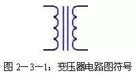
01 transformer diagram
A normally regulated DC power supply uses a power transformer to change input voltage to downstream circuit. The power transformer consists of a primary winding, a secondary winding and a steel core. The primary winding is used to input AC voltage of power supply, and secondary winding outputs required AC voltage.
In simple terms, a power transformer is a device for converting electrical → magnetic → electrical. That is, primary alternating current is converted into a closed alternating magnetic field of iron core, and magnetic field lines cross secondary coil to create a variable electromotive force. When secondary circuit is connected to a load, circuit is closed and an alternating current flows through secondary circuit. The transformer electrical diagram symbol is shown in Figure 2-3-1.
02 rectifier circuit
After being converted by transformer, it is still AC, which must be converted to DC before it can be fed into downstream circuit. This conversion circuit is a rectifier circuit. In a regulated DC power supply, single conductance characteristic of a diode is used to rectify AC and reverse direction to DC.
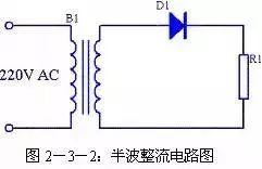
(1) Half-wave rectifier circuit
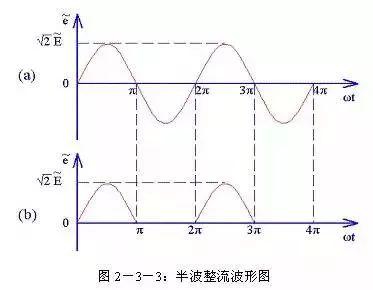
Scheme of half-wave rectification is shown in fig. 2-3-2. Among them, B1 is a power transformer, D1 is a rectifier diode, and R1 is a load. The secondary voltage B1 is a sinusoidal voltage whose direction and magnitude change with time, waveform is shown in Figure 2-3-3(a). The period from 0 to π is positive half-cycle of this voltage. At this time, upper end of secondary winding B1 is positive and lower end is negative, diode D1 conducts forward, supply voltage is applied to load R1, and current flows through load R1;
The period from π to 2π is negative half-cycle of this voltage. At this time, upper end of secondary winding B1 is negative and lower end is positive, diode D1 is reversed, there is no voltage. is applied to load R1, and no current flows through load R1. Repeat above process in successive cycles such as 2π~3π, 3π~4π so that negative half-cycle waveform of power supply is “cut off” and a unidirectional voltage is obtained. Figure 2-3-3(b). Because magnitude of resulting voltage waveform does change with time, we call it DC ripple.
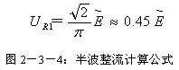
Assuming that secondary voltage B1 is equal to E, voltage across load R1 in ideal state can be obtained by following formula:
Reverse peak voltage of rectifier diode D1:
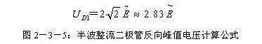
Because half-wave rectifier circuit uses only positive half-cycle of power supply, utilization efficiency of power supply is very low, so half-wave rectifier circuit is only used in a few cases, such as high voltage. and low current, and is rarely used in general power circuits.
(2) Full-wave rectifier circuit
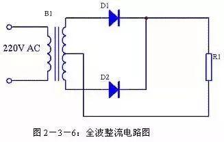
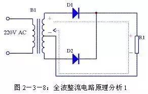
Because efficiency of half-wave rectification circuit is low, people naturally think of using negative half-cycle of power supply to have a full-wave rectification circuit. Figure 2-3-6 shows circuit diagram of full-wave rectification. Compared with half-wave rectification circuit, full-wave rectification circuit uses an additional rectifying diode D2, and a middle tap is added to secondary winding of transformer B1. This circuit is two combined half-wave rectification circuits.
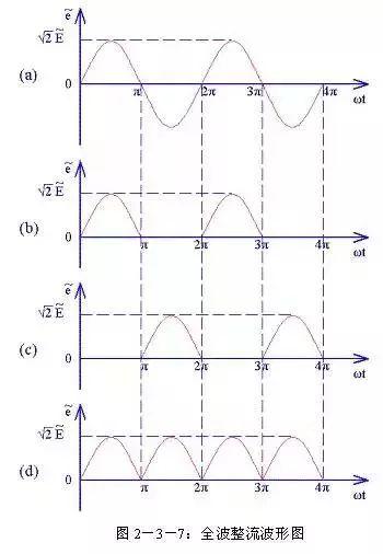
During period from 0 to π, upper end of secondary of B1 is positive and lower end is negative, D1 is forward-conducting, power supply voltage is applied to R1, and voltage at both ends of R1 is positive and lower end is negative. The waveform is shown in fig. 2-3-7. As shown in (b), its current is shown in fig. 2-3-8;
During a period of π to 2π, upper end of secondary of B1 is negative and lower end is positive, D2 conducts forward, and supply voltage is applied to R1. The voltage at both ends of R1 is still positive at upper end and negative at lower . The waveform is shown in Figure 2-3-7(c), its current is shown in Figure 2-3-9.
Repeat above process in subsequent cycles such as 2π~3π, 3π~4π, so that voltage of two positive and negative half-cycles of power supply is rectified by D1 and D2, and then added to both ends of R1. respectively, and voltage received on R1 is always positive, negative down, its shape is shown in fig. 2-3-7(d).
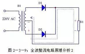
Assuming that secondary voltage B1 is equal to E, voltage across load R1 in ideal state can be obtained by following formula:

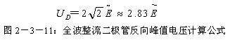
The reverse peak voltage of rectifier diodes D1 and D2 is:
The current flowing through each rectifier diode in full-wave rectification is only half load current, which is half that of full-wave rectification.
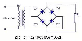
(3) Bridge rectifier diagram
Since full-wave rectifier circuit requires a special transformer, it is more difficult to make it, so bridge rectifier circuit appeared. This rectification circuit uses a conventional transformer, but uses two more rectifier diodes than full-wave rectification. Since four rectifier diodes are connected in a bridge, this rectifier circuit is called a bridge rectifier circuit.
It can be seen from Figure 2-3-13 that during positive half-cycle of power supply, upper end of secondary winding B1 is positive and lower end is negative, rectifier diodes D4 and D2 are turned on. , and current flows from upper end of secondary of transformer B1 through D4, R1, D2, returns to lower end of secondary of transformer B1;
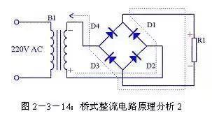
It can be seen from Figure 2-3-14 that in negative half-cycle of power supply, lower end of secondary winding B1 is positive and upper end is negative, rectifier diodes D1 and D3 are turned on. , and current flows from lower end of secondary winding of transformer B1 through D1, R1, D3, returns to upper end of secondary winding of transformer B1. The voltage across resistor R1 is always positive up and negative down, and its shape follows that of a full-wave rectifier.
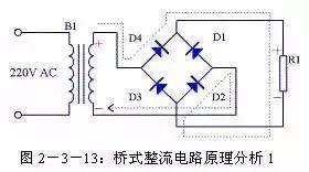
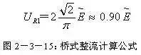
Assuming that secondary voltage B1 is equal to E, voltage across load R1 in ideal state can be obtained by following formula:
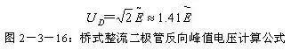
The reverse peak voltage of rectifier diodes D1 and D2 is:
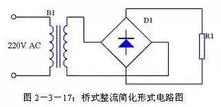
The current flowing through each rectifier diode in a bridge rectifier circuit is half load current, which corresponds to full-wave rectification. Typically, bridge rectifier circuit is simplified to the form shown in Fig. 2-3-17.
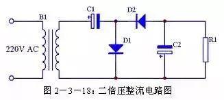
(4) Voltage doubling rectifier circuit
The output voltages of three rectifier circuits shown above are below RMS value of AC input voltage. If output voltage must be higher than RMS value of AC input voltage, a voltage doubling circuit can be used. use as shown in Fig. 2-3-18.
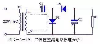
From Figure 2-3-19, it can be seen that in positive half-cycle of power supply, upper end of secondary winding of transformer B1 is positive and lower end is negative, D1 is on, D2 is off, C1 is charging through D1, and voltage at both ends of C1 is close to B1 times after charging. Peak value of step voltage, direction is positive at left end and negative at right end;
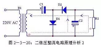
From Figure 2-3-20, it can be seen that in negative half-cycle of power supply, upper end of secondary winding of transformer B1 is negative, and lower end is positive, D1 is off, D2 is off. on, C2 is charging through D1, and voltage at both ends of C2 is close to voltage of C1 after charging. Since load R1 is connected in parallel with C1, when R1 is large enough, voltage across R1 is close to twice secondary voltage of B1.
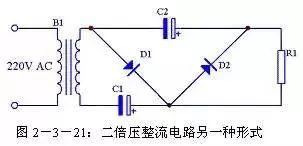
There is another way to draw a dual voltage rectifier circuit, as shown in Figure 2-3-21. Its principle is exactly same as in Figure 2-3-18, but expression form is different.
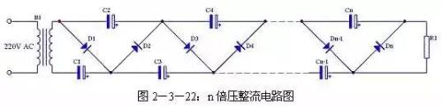
The dual voltage circuit can also be easily extended to n dual voltage circuit, specific circuit is shown in Figure 2-3-22.
Filter Outline 03
After rectifying AC current, a pulsating DC current is obtained. Such a DC power supply cannot be used directly as a power supply for electronic circuits due to large AC ripple it contains. The filter circuit can significantly reduce this AC ripple component, making rectified voltage waveform smoother.
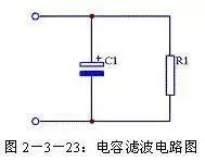
(1) Capacitor filter circuit
The capacitor filter circuit is shown in Figure 2-3-23. The capacitor filter circuit uses principle of charging and discharging a capacitor to achieve a filtering effect. In rising part of DC pulse signal, capacitor C1 is charged, and charging rate is very fast because charging time constant is very small;
In downstream part of DC pulse signal, capacitor C1 is discharged, and discharge rate is very slow due to large discharge time constant. Charging starts again when C1 is not completely discharged. Thus, filtering effect is realized by repeatedly charging and discharging capacitor C1. The voltage waveform at both ends of filter capacitor C1 is shown in Figure 2-3-24(b).

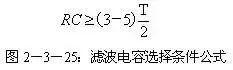
When choosing a filter capacitor, following conditions must be met:
(2)Inductor filter circuit
See rice. 2-3-26 for a schematic diagram of an inductive filter. The inductor filter circuit uses reverse electromotive force of pulsating DC inductance to achieve filtering effect. The larger inductance, better filtering effect. The inductive filter circuit has better load capacity and is mainly used in cases where load current is large.

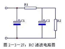
(3) RC filter circuit
Use two capacitors and one resistor to form an RC filter circuit, also known as a π-type RC filter circuit. See Figure 2-3-27. Due to addition of resistor R1 to this filter circuit, AC ripple is distributed across resistor R1. The larger R1 and C2, better filtering effect will be, however, if R1 is too large, voltage drop will be too large and output voltage will be reduced. Usually R1 should be much smaller than R2.
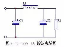
(4) LC filter circuit
Compared with RC filter circuit, there is also an LC filter circuit that combines advantages of low ripple of capacitive filter circuit and high load capacity of inductive filter circuit. Its schematic diagram is shown in fig. 2-3-28.
(5) Active filter chain
When a high filter effect is required, filter effect can be improved by increasing capacitance of filter capacitor. However, limited by volume of capacitor, it is not possible to increase capacitance of filter capacitor indefinitely, and an active filter circuit can be used at this time.
Scheme is shown in fig. 2-3-29, where resistor R1 is base bias resistor of transistor T1, capacitor C1 is base filter capacitor of transistor T1, and resistor R2 is base bias resistor of transistor T1. load. This circuit actually increases capacitance C1 by a factor of β due to amplifying effect of triode T1, which is equivalent to connecting (β+1) capacitor C1 for filtering.
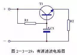
In Figure 2-3-29, C1 can be selected from tens of microfarads to hundreds of microfarads, R1 can be selected from hundreds of ohms to several thousand ohms. The specific value may be determined according to value of β T1. The value of R can be slightly higher if collector-emitter voltage (UCE) of transistor T1 is guaranteed to be greater than 1.5 V. When choosing T1, consider that power dissipation of PCM must be greater than UCEI. If a large amount of heat is generated during operation, you need to add a heatsink.
The active filter circuit belongs to secondary filter circuit, and pre-stage must have a filter circuit such as a capacitive filter, otherwise it cannot work normally.
03 Brief description of rectifier filter circuit
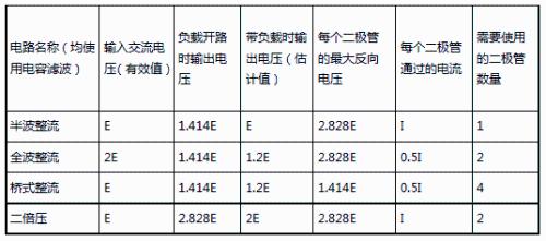
(1) Comparison of characteristics of commonly used rectifier circuits
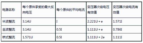
Note: U is voltage value at both ends of load, I is current value at load, e is voltage drop across the rectifier diode, typically 0.7V.
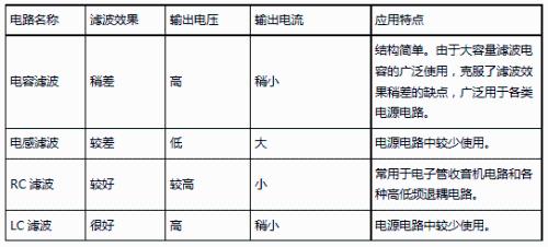
(2) Performance comparison of conventional passive filter circuits
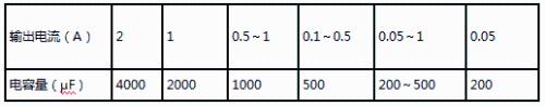
(3) Relationship between output current of capacitor filter circuit and filter capacitance
(4) Calculation table for commonly used rectifier filter circuits
Related
- Haberdashery|One article to understand 4 kinds of rectifier circuits and 5 kinds of filter circuits
- One article eats up all rectifier and filter circuits
- One article to understand design of DC power supply circuit modules.
- A little knowledge of power circuits: will help you understand difference between source current and drain current.
- An article to understand "advantages" and "cons" of solid capacitors
- Summary of questions and answers on basics of analog circuits
- Experience in recognition of circuit diagrams of electronic circuits and method of circuit analysis
- There are several types of MOS lamp drive circuits, you will understand after reading.
- (Dry goods exchange) Eight basic circuits of analog circuits
- How many types of MOS lamp drive circuits are there? I will understand after reading
Hot Posts
 How to distinguish induction from leakage, we will teach you three tricks! Ordinary people can also learn super practical
- What is drowning in gold? Why Shen Jin?
- This is a metaphor for EMI/EMS/EMC that can be understood at a glance.
- How many types of pads have you seen in PCB design?
- Summary of Common PCB Repair Techniques
- What is three anti-paint? How to use it correctly?
- Knowing these rules, you will not get confused looking at circuit diagram.
- How to make anti-interference PCB design?
- Can diodes do this?