Location:Home Page > Archive Archive
Summary of questions and answers on basics of analog circuits
2023-04-02【Archive】
1. What is content of Kirchhoff's theorem?
a) Kirchhoff's current law: at any node in circuit, algebraic sum of currents flowing into and out of node is zero. b Kirchhoff's voltage law: In any closed circuit in a circuit, algebraic sum of the voltage is zero.
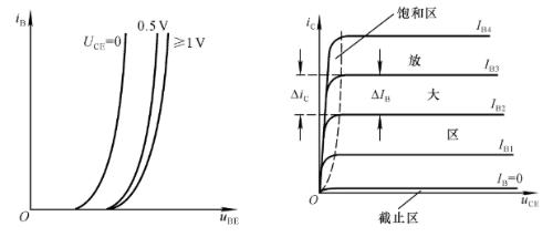
2. Thévenin's theoremA two-terminal circuit with an independent source, a linear resistance, and a controlled source is equivalent to ideal one for both terminals. The series internal resistance model of a voltage source. The value of its ideal voltage source is open circuit voltage of two terminals of an active bipolar circuit, and series internal resistance is equivalent resistance between two terminals when all independent sources inside are zero. 3. Characteristics of triode curve
4. Describe concept of feedback circuits and list their applicationsFeedback: In electronic systems, some or all of output signal (current or voltage) in an amplifying circuit is a process. influencing input value of amplifier circuit through some form of feedback sampling network; and influencing input circuit in some way.
Feedback types: negative voltage feedback, negative current feedback, negative feedback parallel voltage, negative feedback parallel current.
Negative feedback has four effects on amplifier performance:1) Improves gain stability. Due to changes in external conditions (T°C, Vcc, device aging, etc.), increase will decrease. change, and its relative change The smaller value, higher stability. 2) Reduce non-linear distortion and noise. 3) Changed input impedance Ri and output impedance Ro of amplifier. 4) Effectively expand bandwidth of amplifier.
Negative voltage feedback characteristics: The output voltage of circuit tends to remain constant. Characteristics of negative current feedback: The output current of circuit tends to remain constant.
General principles for introducing negative feedback:1) In order to stabilize static operating point of amplifier circuit, negative DC feedback should be introduced to improve dynamic performance of amplifier. circuit needs to introduce negative AC feedback (in polarity of frequency band).
2) If internal resistance of signal source is low or it is necessary to increase input resistance of amplifier circuit, a serial negative feedback should be introduced; if internal resistance of signal source is high, or it is required to reduce input resistance, introduce and connect feedback.
3) According to requirements of output power load or output impedance of amplifying circuit, decide whether to introduce negative voltage feedback or current feedback. If load requires a stable signal voltage or output impedance is low, negative voltage feedback should be introduced; if load needs a stable signal current or output impedance is high, negative current feedback should be introduced.
4) When signal conversion is required, appropriate configuration should be selected according to functions of four types of negative feedback amplifier circuits. For example, when it is required to implement conversion of a current-voltage signal, a parallel negative voltage feedback should be introduced into amplifying circuit. 5. The difference between an active filter and a passive filterPassive filter: This circuit is inMainly composed of passive components R, L and C. Active filter: Consisting of an integrated operational amplifier and R, C, it has advantages of no inductance, small size and light weight. The open-loop voltage gain and input impedance of integrated op-amp is high, and output impedance is small. After active filter circuit is formed, it also has a certain voltage gain and buffering effect. However, bandwidth of built-in operational amplifier is limited, so it is difficult to make operating frequency of current active filter circuit very high. 6. What is a differential mode signal? What is an in-phase signal? Draw structure of a differential circuitTwo pairs of signals of same magnitude and opposite polarity are called differential mode signals. When a differential amplifier circuit supplies a differential mode signal (uil = -ui2) to input, it is called a differential mode input. Two pairs of signals of same size and same polarity are called common-mode signals. When a differential amplifier circuit supplies a common mode signal (uil = ui2), it is called a common mode input. In a differential amplifier, useful signal is input as a differential mode, and interference signal is input as a common mode signal, so interference signal will be very weakly suppressed.
7. Comparison between FET and FETa) When environmental conditions change a lot, it is more appropriate to use a FET. b. Field effect tubes are often used as preamplifiers to improve input impedance of instruments and equipment and reduce noise. c FETs have lower gain capabilities than transistors. d. The process is simple, chip area is small, and it is suitable for large-scale integrated circuits. It is widely used in pulse digital circuits. 8. Basic amplifier circuit principlesa) The emitter junction is forward biased and collector junction is reverse biased. b. The connection of input circuit must provide maximum possible load of input signal to input of amplifier without losses. c. The connection of output circuit must provide maximum possible transfer of output signal to load. 9. Gain Achievement Conditionsa) The transistor must be biased in gain region. The emitter junction is forward biased and collector junction is reverse biased. b. Set static operating point correctly so that entire waveform is within magnified area. c The input circuit converts changing voltage into a changing base current. d. The output circuit converts changing collector current into a changing collector voltage and outputs AC signal only after capacitor filtering. 10. Requirements forpower metera) Output power should be as high as possible. b.High efficiencyc.Low harmonic distortiond.Heat dissipation and protection of transistors11.Frequency compensationThe so-called frequency compensation. It refers to increasing or decreasing power of a signal of a certain frequency to compensate for decrease or increase in frequency generated during signal processing. Commonly used are negative feedback compensation, emitter capacitance compensation, inductance compensation, etc. 12. What is purpose of frequency compensation of an amplifier circuit and what methods are there?
The purpose of frequency compensation in an amplifier circuit is twofold:
One of them is to improve high frequency characteristics of amplifier circuit,
Second, it is necessary to overcome phenomenon of self-excited oscillations, which can occur due to introduction of negative feedback, so that amplifier can work stably.
In amplifying circuit, due to capacitance of transistor junction, high-frequency bandwidth of frequency response of amplifying circuit is often unsatisfactory. To solve this problem, a common technique is to introduce negative feedback into circuit. Then, introduction of negative feedback introduces a new problem, that is, a self-oscillation phenomenon will appear in negative feedback circuit, so in order for amplifying circuit to work normally and stably, it is necessary to perform frequency compensation on amplifying circuit.
Frequency compensation method can be divided into lead compensation and lag compensation. It is basically change in phase-frequency characteristics of open-loop gain of amplifier circuit in high-frequency band by connecting some resistance-capacitive components. At present, most commonly used is phase lock ring. 13. Types of basic amplifying circuits (voltage amplifiers, current amplifiers, slope amplifiers and slope amplifiers), advantages and disadvantages, features of reasons for widespread use of differential structures.
The role of amplifier circuit: The amplifier circuit is one of circuits widely used in electronic engineering, its function is to amplify weak input signal (voltage, current, power) without distortion to a value, required for loading. Amplifier circuit types:(1) Voltage amplifier: input signal is very small, and it is required to obtain a larger output voltage without distortion, also known as a small signal amplifier; (2) Power amplifier: input signal is large, so amplifier must output enough power, also known as a large signal amplifier.
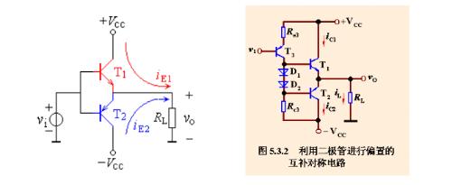
A differential circuit is a circuit that performs such a function. The input terminal of circuit is input of two signals, difference between two signals is effectivethe circuit's input, and circuit's output is amplification of difference between two inputs. Imagine such a scenario, if there is an interference signal, it will create same interference for two input signals, and due to difference between them, effective input interference signal is zero, which achieves goal of anti-common-mode interference. 14. Class A power amplifier, Class B complementary balanced power amplifier, and Class A and B complementary balanced power amplifier, specifications and circuit diagrams.
15. Try to draw a block diagram of a phase locked loop and briefly describe principle. Phase Hold: Lock phase and frequency at a fixed value. PLL: A loop that blocks a phase. The composition of phase locked loop: PD phase detector + frequency divider + LPF loop filter + voltage controlled oscillator, VCO, etc. Phase-locked loop operation principle:1) The output signal of a voltage controlled oscillator is collected and divided by frequency;2) and reference signal is applied to phase detector at input. simultaneously; Compare frequency difference of above two signals, and then output DC pulse voltage;4) Operate VCO to change its frequency;5) After a short time, VCO output will change. be stable with some expectation. Reference signal
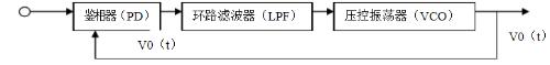
A phase detector is a phase comparison circuit. The input reference signal is compared with VCO output signal, and an error signal representing phase difference is output. After passing through loop filter, harmonic and noise components in error signal are filtered out, and error voltage is calculated. is obtained to control VCO. The frequency of controlled oscillator changes in direction of decreasing frequency difference and phase difference between two signals. Finally, VCO output frequency is equal to frequency of reference signal. 16. What is zero drift? How to suppress zero drift? Zero drift means that when input terminal of amplifier circuit is shorted, there is still a slowly changing voltage at output terminal, that is, output voltage deviates from original starting point and drifts. up and down. Techniques for suppressing zero drift typically include:a) using constant temperature measures;c) using negative DC feedback to stabilize static operating point;d) using RC coupling between or use a specially designed DC modulation and demodulation amplifier. 17. What is a frequency response, how to consider a stable frequency response, briefly describe several ways to change frequency response. Frequency response: Commonly also referred to as frequency response, frequency response, or frequency response, it is a technical metric for measuring adaptability of an amplifier circuit to various frequency input signals.
In amplifying circuit, due to presence of reactive components (such as capacitors, inductors, etc.), there will be a decrease and a phase advance or lag phenomenon will occur. In other words, gain (or amplification) of amplifier circuit and frequency of input signal is a functional relationship, and we call this functional relationship frequency response or frequency response of amplifier circuit.
Basically, frequency response refers to relationship between an amplifier's gain and frequency. Generally speaking, a good amplifier should not only have sufficient gain, but also have good fidelity, that is, harmonic distortion of amplifier should be small, and frequency response of amplifier should be good. "Good" means that amplifier should equally amplify signals of different frequencies.
The reason for frequency response: firstly, frequency of actually amplified signal is not single, and secondly, amplifier has reactive components and reactive coefficients. Due to presence of reactive components in amplifying circuit (such as tube-to-electrode capacitance, circuit load capacitance, distributed capacitance, coupling capacitance, emitter bypass capacitance, etc.), amplifier can have different gains and phase shifts for different frequency components of signal. If amplifier circuit amplifies amplitude of si in different wayssignals of different frequencies, this will cause amplitude distortion; if amplifier circuit creates different phase shifts for signals of different frequencies, this will cause phase distortion. Amplitude distortion and phase distortion are collectively referred to as frequency distortion. Since this distortion is caused by linear reactance components (resistance, capacitance, inductance, etc.) of a circuit, it is not called linear distortion. To realize signal amplification without distortion, it is necessary to study frequency response of amplifier.
The frequency response of an amplifying circuit can be described by a frequency response and a phase response. If frequency response of an amplifying circuit is a straight line parallel to x-axis (or within frequency range of interest, parallel to x-axis), and If phase response is a straight line through origin (or a straight line through origin in frequency range of interest), then frequency response is stable.
The main ways to change frequency response are:1) changing parameters of components of amplifying circuit;2) introducing new components to improve frequency response of existing amplifying circuit. ; 3) The new amplification circuit is connected in series with original amplification circuit, forming a multi-stage amplification circuit. 18. Transistors work in gain region, how to bias emitter junction and collector junction
19. Why would a receiver need to add an AGC scheme. 1) The strength of received signal varies greatly, and difference is large. If you do not add AGC, output signal will fluctuate greatly, which will affect effect. 2) To be able to receive weak signals, receiver gain is always made larger, that is, sensitivity is high, but when receiving strong signals, if channel gain is not adjusted, bad consequences will occur. 20. Name three-point oscillatory circuits of an LC sine-wave generator and draw their circuit diagrams accordingly. Inductive three-point generator and capacitive three-point generator
21. Point out differential op amp, how to perform phase compensation, and draw compensated Bode diagram. As operating frequency increases, amplifier will produce additional phase shift, which can convert negative feedback into positive feedback and cause self-excitation. Performing phase compensation can eliminate high frequency self-excitation. The principle of phase compensation is as follows: in high gain intermediate stage, use a small capacitor C (tens to hundreds of picofarads) to form a parallel voltage negative feedback circuit. Capacitance correction and RC correction can be used to change phase-frequency characteristics and amplitude-frequency characteristics, respectively. 22. For a differential circuit whose output voltages Y+ and Y- are known, find common mode and differential components. If common mode component is Yc and differential mode component is Yd, then output signal is Y+=Yc+YdY-=Yc-Yd< br > > 23. Is it generally better to have more or less input impedance and output impedance of amplifier? Why? In a gain circuit, it is generally desirable that input impedance of gain circuit be high, since it has little effect on signal source. Looking at output end of amplifier circuit, amplifier circuit can be equivalent to a signal source with a certain internal resistance. The signal source's internal resistance is output impedance. It is generally hoped that lower value, better, because it can improve load on amplifier. 24. Principle of regulated DC power supplyFunction: Converting AC voltage into a stable DC voltage of appropriate size
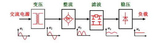
Power transformer: Convert AC mains voltage u1 to a suitable AC voltage u2. Rectifier circuit: converting an AC voltage u2 into a pulsating DC voltage u3. Filter circuit: Converting a pulsating DC voltage u3 into a smooth DC voltage u4. Voltage stabilizer circuit: eliminates influence of mains fluctuations and load changes, and keeps the output voltage uo stable.
25. The composition of integrated circuits of operational amplifiers
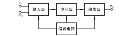
Bias Circuit: Set an appropriate static operating point for amplifier circuits at all levels. Wider use of constant current source circuit. Input stage: often a differential amplifier circuit. It is required that Ri be large, Ad large, Ac small, and input terminal withstand voltage high. It has two inputs, non-inverting and inverting.
Intermediate stage: main amplifier stage, usually a common emitter amplifier circuit, mostly using composite tubes. Sufficient magnification required. Output stage: power stage, mainly using complementary power amplifier circuit or emitter follower. Ro is required little, and maximum undistorted output voltage is as high as possible. 26. Active filterFirst order active low pass filter and first order active high pass filter.
27. Composition and working principle of RC oscillator amplifier circuits3) Frequency selection network: to ensure that output is a single frequency sine wave even if circuit only satisfies its own generation conditions at a particular frequency4) Amplitude stabilization link: Make circuit transition from ½AuF½> 1 to ½AuF½ =1 to achieve a stable oscillation.
Related
- Summary of questions and answers on basics of analog circuits
- Experience in recognition of circuit diagrams of electronic circuits and method of circuit analysis
- ADC basics and comparative analysis of different ADC technologies
- Deep Understanding of Analog Electronics - Analog Electronics Tutorial
- Analysis and comparison of 6 most commonly used DC power supply circuits
- Daniel's Summary: The details and experience of 30 PCB layouts are wonderful.
- Analog electronics 200 questions
- Inventory of 27 functions of capacitors in circuits
- A detailed explanation of role of pull-up resistors on triodes and MOS lamps.
- An interesting summary of PID algorithm full of haberdashery
Hot Posts
 How to distinguish induction from leakage, we will teach you three tricks! Ordinary people can also learn super practical
- What is drowning in gold? Why Shen Jin?
- This is a metaphor for EMI/EMS/EMC that can be understood at a glance.
- How many types of pads have you seen in PCB design?
- Summary of Common PCB Repair Techniques
- What is three anti-paint? How to use it correctly?
- Knowing these rules, you will not get confused looking at circuit diagram.
- How to make anti-interference PCB design?
- Can diodes do this?