Location:Home Page > Archive Archive
Schottky diode principle
2023-03-18【Archive】
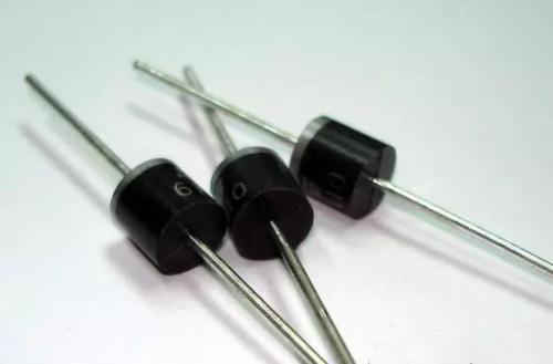
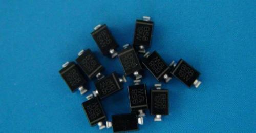
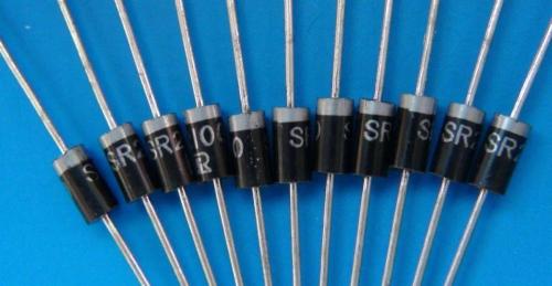
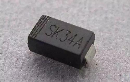
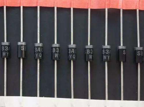
Schottky Diode
The Schottky Diode is named after its inventor, Dr. Schottky, and SBD is short for Schottky Barrier Diode. The SBD is not made by principle of contacting a P-type semiconductor and an N-type semiconductor to form a PN junction, but by a metal-semiconductor junction formed by a metal-semiconductor contact. Therefore, SBD is also called metal semiconductor (contact) diode or surface barrier diode, which is a kind of hot carrier diode.
1 Schottky diode principle
Schottky diodes are precious metals (gold, silver, aluminum, platinum, etc.) A as positive pole and N-type semiconductor B as negative pole. Metal-semiconductor device. Since there are a large number of electrons in an N-type semiconductor and only a small number of free electrons in noble metal, electrons diffuse from high concentration B to low concentration A. Obviously, there are no holes in metal A, and there is no diffusion of holes from A to B. As electrons continue to diffuse from B to A, concentration of electrons on surface of B gradually decreases, and electrical neutrality of surface is destroyed, forming a potential barrier, and its electric field is directed B→A. However, under influence of electric field, electrons in A will also drift away from A → B, thereby weakening electric field generated by diffusion motion. When a space charge region of a certain width is established, drift motion of electrons caused by electric field and diffusion motion of electrons caused by different concentrations reach a relative balance, forming a Schottky barrier.
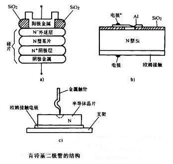
The internal circuit structure of a typical Schottky rectifier is based on an N-type semiconductor substrate on which an N-epitaxial layer with arsenic as a dopant is formed. Materials such as molybdenum or aluminum are used as barrier layer in anode. Silicon dioxide (SiO2) is used to eliminate electric field in edge region and improve tube's withstand voltage. The N-type substrate has very low on-resistance, and its doping concentration is 100% higher than that of H-layer. An N+ cathode layer is formed under substrate to reduce contact resistance of cathode. By adjusting structural parameters, a Schottky barrier is formed between N-type substrate and anode metal, as shown in figure. When a forward bias is applied to both ends of Schottky barrier (the anode metal is connected to positive pole of power supply, and N-type substrate is connected to negative pole of power supply), Schottky barrier layer becomes narrower and its internal resistance becomes smaller; otherwise, if a reverse bias is applied to both ends of Schottky barrier, layer of Schottky barrier will become wider and its internal resistance will become larger.
Summarizing, we can say that structural principle of Schottky rectifier is very different from PN junction rectifier. Usually, a PN junction rectifier is called a junction rectifier, and a metal-to-semiconductor type rectifier is called a Schottky rectifier. Si-Schottky diodes, manufactured using silicon planar technology, have also been released, which allows not only saving precious metals, significantly reducing costs, but also improving constancy of parameters.
2 The benefits of Schottky diodes
SBD has advantages of high switching frequency and low forward voltage, but its reverse breakdown voltage is relatively low, mostly not higher than 60V, and maximum value is only about 100V, which limits its application range. For example, reverse diodes of power switching devices in switching power supply circuits (IMIP) and power factor correction (PFC), high-frequency rectifier diodes above 100V for secondary winding of transformer, high-speed diodes 600V~1.2kV in RCD snubber circuits, and For 600V diodes used to boost the CMC, only Fast Recovery Epitaxial Diodes (FRED) and Ultra Fast Recovery Diodes (UFRDs) are used.
The reverse recovery time Trr UFRD is also over 20 ns, which cannot meet needs of 1-3 MHz SMPS in areas such as space stations. Even for a 100kHz hard-switched SMPS, due to large conduction losses and switching losses of HPJD, case temperature is high, and a large heat sink is required, which increases size and weight of SMPS, which does not meet miniaturization and thinning requirements of development trend. Therefore, development of high voltage SBDs above 100 V has always been a subject of research and attention. In recent years, SBD has made breakthrough progress, 150V and 200V high-voltage SBDs have been listed, and over 1kV SBDs have been successfully developed from new materials, bringing new vitality and vitality to its application.
3 disadvantages of Schottky diodes
The biggest disadvantage of Schottky diodes is low reverse bias voltage and large reverse leakage current. For silicon and metal Schottky diodes, their rated reverse bias withstand voltage is only up to 50V, and reverse leakage current value has a positive temperature characteristic , which tends to rapidly increase with increasing temperature. When calculating physically, it is necessary to pay attention to hidden danger of thermal runaway. To avoid above problems, reverse bias voltage of Schottky diodes in actual use will be much less than its nominal value. However, technology of Schottky diodes has also improved and their reverse bias voltage rating can reach a maximum of 200V.
4 The difference between Schottky diodes and conventional diodes
The main feature of Schottky diodes is a low voltage drop in forward direction and a short reverse recovery time. Schottky diodes have a low turn-on voltage and little charge storage effect, making them suitable for high frequency operation. For same current, its forward voltage drop is much less than conventional diodes. It also has characteristics of low loss, low noise, high detection sensitivity, stability and reliability, etc. It is used in microwave communication and radar for frequency mixing, detection, modulation, frequency multiplication, super high switching speed and low frequency . - noise amplification.
So, most obvious differences between Schottky diodes and conventional diodes are as follows:
1. The forward voltage drop across Schottky diodes is lower than conventional diodes, so power consumption is low.
2. The reverse recovery time of Schottky diodes is shorter than conventional diodes, so operating frequency is higher.
3. The reverse withstand voltage of Schottky diodes is lower than conventional diodes, typically below 200V.
4. Schottky diodes carry more current than conventional diodes.
5. Schottky diodes have less junction capacitance than conventional diodes.
6. Schottky diodes can pass high frequency current.
Related
- Schottky diode principle
- Do you know 4 characteristics of Schottky diodes?
- Commonly Used Diode Circuits Essential for Engineers
- Diode switching circuit and troubleshooting, one complete wizard
- What is difference between TVS tube and zener diode?
- Principle of electronic switch to realize overcurrent protection
- Leaving aside calculations, in principle workflow of LLC
Hot Posts
 How to distinguish induction from leakage, we will teach you three tricks! Ordinary people can also learn super practical
- What is drowning in gold? Why Shen Jin?
- This is a metaphor for EMI/EMS/EMC that can be understood at a glance.
- How many types of pads have you seen in PCB design?
- Summary of Common PCB Repair Techniques
- What is three anti-paint? How to use it correctly?
- Knowing these rules, you will not get confused looking at circuit diagram.
- How to make anti-interference PCB design?
- Can diodes do this?