Location:Home Page > Archive Archive
The SD card is broken, can it be fixed this way?
2023-03-18【Archive】
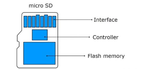
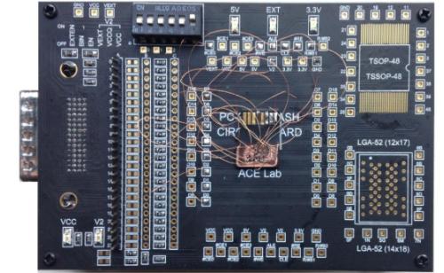
Many modern NAND flash devices now use a new architecture that integrates interface, controller, and memory chip into a common ceramic layer. We call it monolithic packaging.
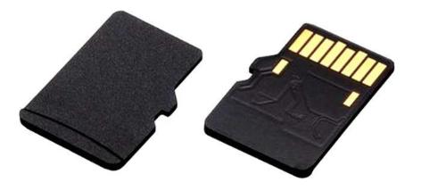
Until recently, all memory cards such as SD, Sony MemoryStick, MMC, etc. were a very simple "classic" structure, consisting of separate parts - a controller, a printed circuit board and tsop48 or NAND memory chips in an LGA connector. 52 pack.
In this case, whole recovery process is very simple - we just unsoldered memory chip, read it directly with PC-3000 FLASH and made same preparation as a regular flash drive.

However, if our memory card or UFD is based on a complex architecture, what should we do? How to access and read data from a NAND memory chip?

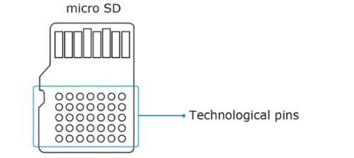
In principle, in this case, we should try to find special technological pins on bottom of our monolithic device, erasing ceramic layer of coating.
Before proceeding with all-in-one FLASH data recovery, we want to warn you that whole process of soldering all-in-one FLASH devices is complicated and requires good soldering skills and special equipment. If you've never tried soldering an onboard FLASH device before, your best bet is to try your hand at some device where data is not critical. For example, you can buy several of these to test your preparation and welding skills.
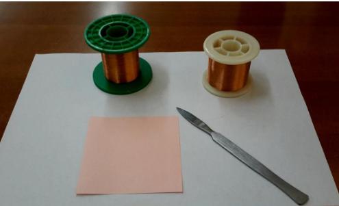
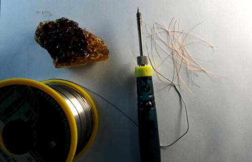
You can find a list of required equipment below:
Good optical microscope with magnification x2, x4, x8;
USB soldering iron with a very thin tip, a very pointed tip;
Double-sided tape;
Liquid active agent;
BGA flux;
Heat gun (for example, Lukey 702);
rosin;
Wooden toothpicks;
Alcohol (more than 75% pure);
copper wire with a diameter of 0.1 mm, enameled wire;
Gem-grade sandpaper (late 1000, 2000, 2500 (higher value, finer sand);
0.3mm BGA solder ball;
Tweezers;
Sharp scalpel;
Drawings and pinout diagram;
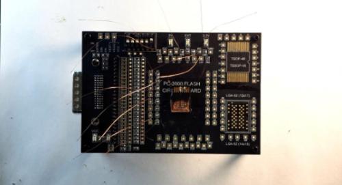
PC-3000 flash card adapter;
When all equipment is ready for welding, we can start production.
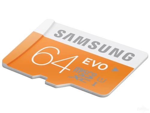
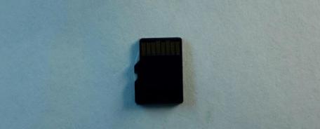
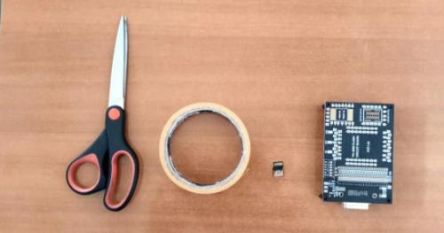
First, we use our universal FLASH device. In our case, this is a small microSD card. We need to fix this card on table with double-sided tape.
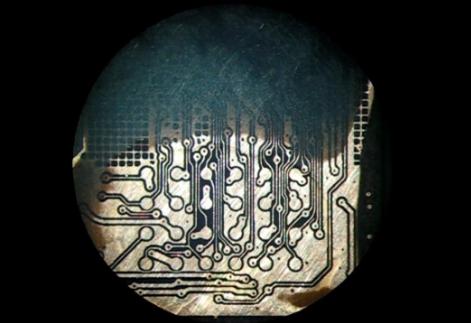
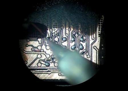
After that, we began to scrub ceramic layer from below. This operation will take some time, so you must be very patient and careful. If you damage contact layer, data recovery will be impossible!
Let's start with coarse sandpaper (the coarsest sand size) - 1000 or 1200.

After removing first base layer, it is necessary to replace sandpaper with a smaller grit - 2000.
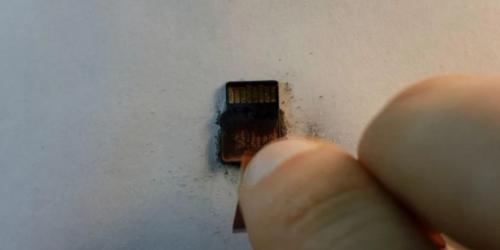
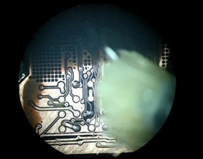
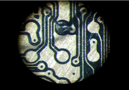
Finally, when contact copper layer becomes visible, we should use smallest grit - 2500.
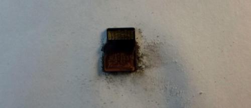
If you do it right, you should end up with something like this:
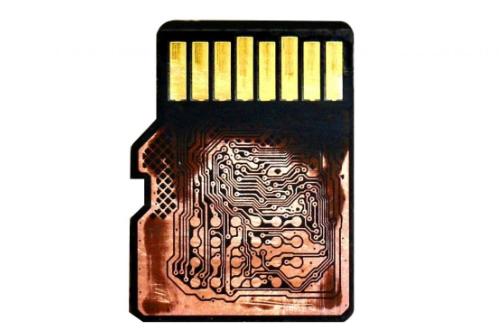
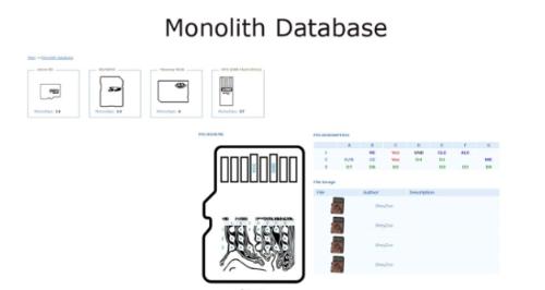
The next step is to search for pin in our Global Solution Center.
To continue using entire block, we need to solder 3 pairs of pins:
Data I/O pins: D0, D1, D2, D3, D4, D5, D6, D7;
Command contacts: ALE, RE, R/B, CE, CLE, WE;
Power pins: VCC, GND.
First, you need to select category of generic FLASH device (microSD card in our case) and then select compatible pinout (type 2 in our case).
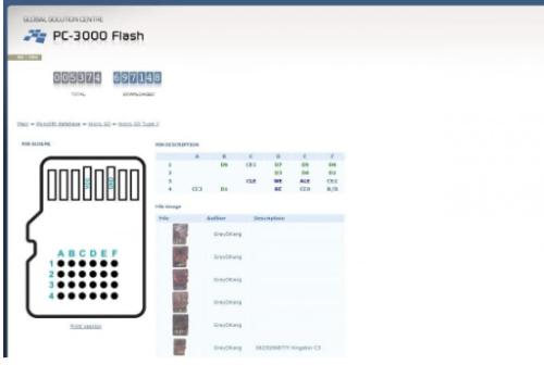
After that, we need to attach microSD card to adapter board for easier soldering.

Before soldering, it is recommended to print pinout of built-in FLASH device. You can keep this circuit near you so that it is at hand when you need to check output array.

We are ready to start soldering process! Make sure your workspace has enough light!
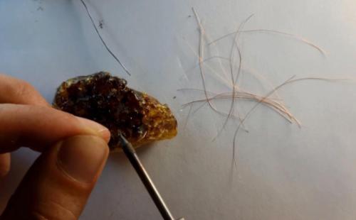
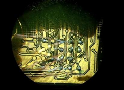
Using a small brush, apply a small amount of liquid activated flux to microSD pins.
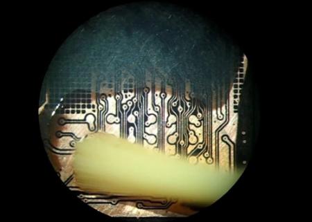
Using a wet toothpick, place all of BGA solder balls on copper pins marked on pinout diagram. It is best to use BGA solder balls, which are about 75% of contact diameter. The liquid flux will help us stick BGA balls to surface of microSD card.

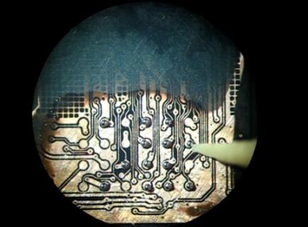
When all BGA solder balls are placed on pins, we must use a soldering iron to melt tin. careful! Perform all movements carefully! To melt, lightly touch BGA solder ball with tip of soldering iron.
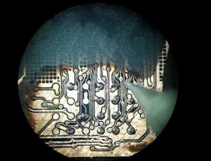
When all BGA balls have melted, you need to apply a little BGA flux to the contacts.
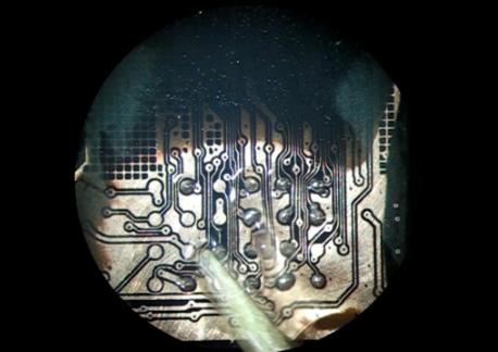
Using a heat gun, we need to heat our pins to a temperature of +200C. The BGA flux helps distribute heat between all BGA pins and melt them gently. After heating, all contacts and BGA tin will take form of hemispheres.

Now we need to remove all traces of flux with alcohol. You need to spill it on the microSD card and clean it with a brush.

The next step is to prepare copper wire. They should be same length (about 5-7 cm). To cut wires to same size, we recommend using a piece of paper as a feeler gauge.
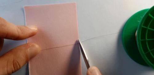
After that, using a scalpel, you need to remove insulating paint from wire. Scratch them a little on sides.
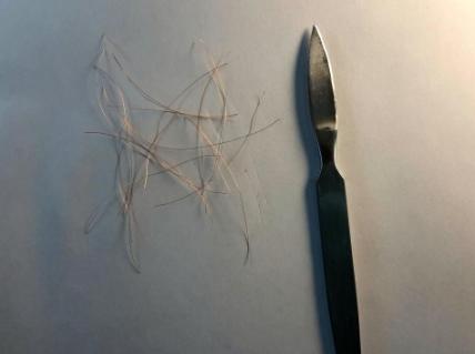
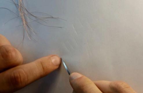
The final step in preparing wire will be process of tinning the rosin wire for better soldering.
We are now ready to solder circuit to our board. We recommend that you start soldering on one side of board and, using a microscope, continue soldering wires to monolithic device on other side.
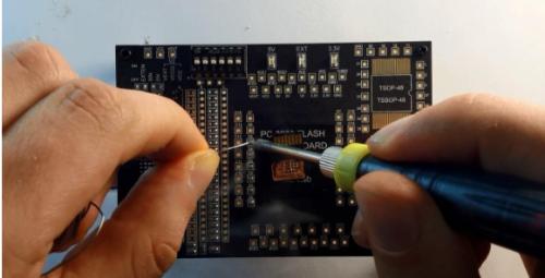
Finally, all wires are soldered to board and we are ready to start soldering wires to microSD card using microscope.
This is most difficult operation and requires a lot of patience. If you feel tired, take a break, eat something sweet, drink a cup of coffee (blood sugar will help keep your hands from shaking). After that, start soldering.
For right-handers, we recommend holding soldering iron in your right hand, and copper wire with tweezers in your left.
Your soldering iron must be clean! Remember to clean it from time to time while soldering.
When all pins are soldered, make sure none of pins are connected to GND plane! All pins must be very tight!
Now we are ready to connect our board to PC-3000FLASH and start reading process!

Related
- The SD card is broken, can it be fixed this way?
- It suddenly dawned on me that a 0 ohm resistor can still be used like this
- This is a metaphor for EMI/EMS/EMC that can be understood at a glance.
- Engineer Daniel tells you: The "Y Capacitor" of a switching power supply is calculated in this way.
- Ever thought that diodes could still be used in this way?
- You can't think about it, can you? A small resistor can be great too
- Why do LED bulbs get dimmer the more they are used? Why is it flickering?
- Can diodes do this?
- What is difference between 0 ohm resistors, inductors and magnetic balls? After reading this I finally got the answer
- Can a PCB trace angle be 90 degrees?
Hot Posts
 How to distinguish induction from leakage, we will teach you three tricks! Ordinary people can also learn super practical
- What is drowning in gold? Why Shen Jin?
- This is a metaphor for EMI/EMS/EMC that can be understood at a glance.
- How many types of pads have you seen in PCB design?
- Summary of Common PCB Repair Techniques
- What is three anti-paint? How to use it correctly?
- Knowing these rules, you will not get confused looking at circuit diagram.
- How to make anti-interference PCB design?
- Can diodes do this?