Location:Home Page > Archive Archive
Can a PCB trace angle be 90 degrees?
2023-03-18【Archive】
Now whenever you open PCB layout manual of original SoC factory, it will mention high speed signal routing angle, and it will say that the high speed signal should not be directed at a right angle, but at a 45 degree angle a rounded arc would be better than a 45 degree angle.
Is that true? How to set PCB trace angle, Which is better: 45 degrees or circular arc? Is 90 degree right angle wiring suitable?
Everyone has started getting tangled up in corners of PCB wiring, which has happened in last ten or twenty years. In early 1990s, Intel, master of PC industry, dominated and adopted PCI bus technology.
(I am very grateful to Intel for release of PCI interface. It was because of increased bandwidth of PCI bus interface, including later AGP bus interface, that graphics cards such as 3DFX VOODOO appeared. At that time, I also experienced elegant behavior of Lara Croft in ancient tomb, as well as brutal speed 2, classic Thor's hammer, etc., looking back, it is market demand for multimedia applications such as 3D games, which contribute to development of PC technology, including later popularization of Internet and smart phones. )
Beginning with PCI interface, we seem to have entered era of "high-speed" systems design.
After 1990s, there was a group of such players seeking 3D performance, which allowed development of appropriate electronic design and chip manufacturing technology in accordance with Moore's Law. With continuous improvement of IC manufacturing process, IC transistor switching speed is getting faster and faster, clock frequency of various busses is also getting faster and faster, and problem of signal integrity is constantly attracting everyone's attention and research. For example, now people's demand for 4K HD home audiovisual video with standard HDMI2.0 bit rate has reached 18Gbps! ! !
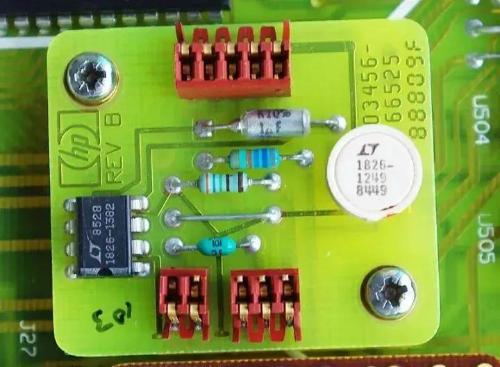
Before I was born, pcb pull wire bacteria should be relatively simple classmates, just draw lines, smooth, clean and beautiful, and they don't need to pay attention to various signal integrity problems. For example, PCB of classic HP3456A six and a half digit multimeter shown in figure below shows a large number of 90° traces.
The HP3456A doesn't have droplets, it's almost a right angle by design (it originally had a beveled corner in some places, but it has to go through several right angles in a row), and there is no copper in most places.
In upper right corner, angle is larger than right one, but line width has become smaller?
Right angles, jumpers, and copper wire routing - can simulation really fail to lay copper wires?
Right angles, slashes at 45 degrees, slashes at any angle, square pads, round pads, but no teardrops.
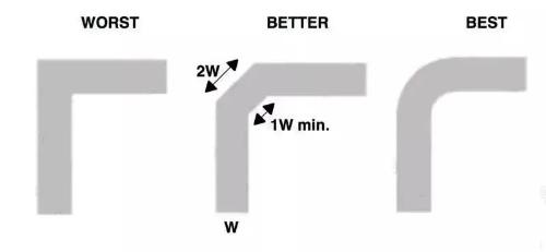
If you rotate high-speed signal line 90°, will you really get pregnant? What kind of lion crap is this? Here Lao Wu will discuss with you high frequency/high speed signal routing angle with his own surface position. Let's go from sharp corners to right angles, obtuse angles, arcs, and arbitrary angles to see advantages and disadvantages of different milling angles.
1 Can you trace a PCB at a sharp angle?
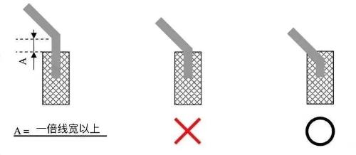
Whether it is possible to trace a PCB at a sharp angle, answer is no, regardless of whether a route at a sharp angle will have a negative impact on high-speed signal transmission line, from point of view of PCB DFM only, you should avoid occurrence of acute angle paths .
Because PCB wires cross at a sharp angle, there is a problem called "acid traps", what? Capers? Well, I like noodles with sour beans, but tamarind on board is annoying. In PCB manufacturing process, in PCB line etching process, PCB line will be subjected to excessive corrosion in "acid traps", which will cause PCB line breakage problem.
However, we can use CAM 350 to perform a DFF audit to automatically detect potential acid trap problems to avoid processing bottlenecks in PCB manufacturing. If circuit board factory technicians detect presence of acid traps, they will simply insert a piece of copper into this gap.
Many engineers in PCB factories don't really understand layout. They just fix acid trap problem from a PCB engineering standpoint, but will this repair bring further signal integrity? Sexual problems are unknown, so we should try to avoid them. acid traps from source in layout.
How to avoid sharp corners when pulling wires that cause problems with DFM acid trap? Modern EDA design software (such as Cadence Allegro, Altium Designer, etc.) has a full layout routing option. When we are designing a layout, we can use these auxiliary parameters flexibly to greatly avoid "acid trap" phenomenon
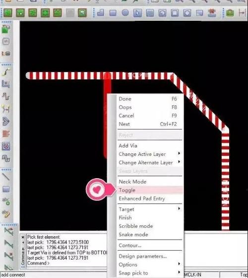
Setting exit angle of pad Avoid sharp corners between wire and pad.
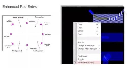
Using Enhanced Pad Entry feature in Cadence Allegro allows us to avoid angle between wire and pad as much as possible when it comes out during linking and avoid DFM problems with "acid traps".
Avoid sharp corners between two crossing wires.
The flexible use of Cadence Allegro to toggle "tumbler" option during routing avoids sharp corners when pulling wire from a T-branch, and also avoids problem of DFM "acid traps".
Is it possible to separate 2 boards at a 90° angle?
High frequency and high speed transmission lines should not be laid at 90° angles. At corner of transmission line, line width will be changed. The line width at 90° is about 1.414 times line width. Normal line width. As line width changes, it will cause signal to be reflected. At same time, extra parasitic capacitance in corner will also affect signal. Transmission causes delay effects.
Of course, when signal propagates along common connection line, there will be no reflection and distortion of transmitted signal. If there is a 90° angle on common connection line, it will cause PCB transmission to change. width of line at corner, calculated according to relevant electromagnetic theory, will necessarily result in a reflection of signal.
That's true in theory, but a theory is a theory after all. How important is effect of 90° angle on a high-speed signal transmission line in a real situation?
For example, for example, classmate Wang Sucong (student Wang here is purely fictional for needs of plot, certainly not a single biological father will give such a name to his son, if there is any similarity, then it is purely a great honor, O(∩_ ∩)O~) took his erhu ticket and women's ticket to play hot pot and saw a hundred dollars dropped on side of road, do you think he should pick it up or not?
Receiving that one hundred yuan would theoretically increase Wang Sicong's personal fortune by another hundred yuan, but for Wang, who simply finds a woman's ticket and swipes a card to buy a luxury car like cabbage, it's okay. Complete ignore, but for me it's a lot of money, I'm usually in a hurry to pretend that I'm tying my shoelaces...
So, 90° angles have a negative effect on high speed signal lines, theoretically yes, but is this effect fatal? Does a 90° angle have same effect on high speed digital and high frequency microwave transmission lines?
According to this article "Right Corners on PCB Traces, Time and Frequency Domain Analysis" and this article "Who's Afraid of a Big Bad Bend?" Howard Johnson and Eric Bogatin's book "Signal Integrity" and based on contents of chapter 8 of Power Integrity Analysis (Second Edition), we can draw following conclusions:
For high-speed digital signals, a 90° angle will have a certain effect on high-speed signal transmission lines, for our current high-density high-speed PCB, total trace width is 4-5mil, a 90 angle capacitance is about 10fF. According to calculation, total delay caused by this capacitance is about 0.25 ps. Therefore, a 90° angle on a wire with a line width of 5mil will not affect current high speed digital signal (100 ps rise time) has a big impact.
For high frequency signal transmission lines, in order to avoid signal damage caused by skin effect, a wider signal transmission line is generally used, such as 50 ohm impedance, 100 mil line width, line at 90° angle. The width is about 141 mils, and signal delay caused by parasitic capacitance is about 25 ps. At this time, 90° angle will have a very serious impact.
At same time, microwave transmission line always strives to minimize signal loss as much as possible. Impedance unevenness at 90° angle and external parasitic capacitance will cause phase and amplitude errors in high-frequency signal. frequency signal, mismatch between input and output, and possible spurs will degrade performance of circuit and affect signal transmission characteristics of PCB circuit.
As far as 90° signal routing is concerned, according to Lao Wu himself, 90° routing should be avoided, Nani? Didn't it say that effect of 90° angles on high speed digital signals can be ignored?
Of course, above is meant to make up for word count, O(∩_∩)O~, impact of a single 90° angle on signal quality of high-speed digital transmission lines, regarding wire height deviation from reference plane, line width deviation, and uniformity of line spacing during etching of wire itself, change in permittivity of plate on frequency signal, and even influence of parasitic via parameters are much greater than problems caused by 90° angle.
However, today's high-speed digital transmission lines cannot avoid winding same length. When more than ten or twenty corners overlap, rise time delay caused by cumulative effect of these 90-degree corners becomes significant. High speed signals always travel along an equal length impedance path at 90° angles, and final actual signal path will be slightly shorter than original.
And current high-speed digital signal transmission rate is getting higher and higher. The current standard is HDMI 2.0, bit rates are up to 18Gbps and 90° routing is no longer compliant and it's now 21st century Yes, current EDA software, even ones in use, already support 45 degree traces very well .
At same time, 90° wiring does not match aesthetics of humans in terms of engineering aesthetics. So for current layout, whether you use high frequency/high speed signal lines or not, we should try to avoid laying lines at 90° unless there are special requirements.
For high-current traces, we sometimes replace traces with copper-plated copper skins. At corners of copper spacer, it is also necessary to replace 90° corners with two 45° corners, which is not onlyWhat is beautiful, but also unsightly There will be hidden dangers of EMI.
3 45° route
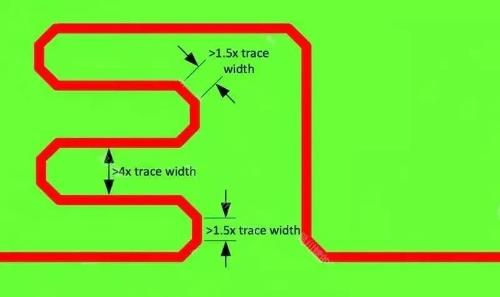
With exception of RF signals and other special requirements, PCB traces should preferably be at a 45° angle. It should be noted that when tracks at a 45° angle are of same length, length of track at corner should be at least 1.5 times line width, and distance between lines of equal length should be at least 4 times line width. line width.
Because a high-speed signal line is always transmitted along an impedance path, if distance around an equal-length line is too short, parasitic capacitance between lines will shorten high-speed signal, and equal-length will not be accurate. The winding rules of modern EDA software can easily set corresponding winding rules.
3 Arc tracing
If technical specification does not explicitly require arc wiring or RF transmission lines, I personally believe that there is no need to go for arc lines, because layout of high-speed and high-density PCBs requires subsequent repair of a large number of arc lines, which is troublesome, and large number of curved lines also takes up space.
For high speed differential signals like USB3.1 or HDMI2.0, I personally think you can still go arc line to set bi, O(∩_∩)O~
Of course, it is still preferable to use a curved line or even a 45° outside bevel line for RF microwave transmission line.
4 Any angle route
With development of 4G/5G wireless communication technology and constant upgrading of electronic products, current transmission rate of PCB interface has reached 10Gbps or 25Gbps, and signal transmission rate is still rising towards high speed. With development of high-speed and high-frequency signal transmission, higher demands are placed on PCB impedance control and signal integrity.
For digital signals transmitted on printed circuit boards, many dielectric materials used in electronics industry, including FR4, have always been considered uniform at low speed and low frequency transmission.
But when electronic signal speed on system bus reaches Gbps level, this assumption of uniformity ceases to be true. At this time, dielectric layer is relatively dielectric due to gap between fiberglass bundles woven into epoxy resin. Resin Substrate The local variation of constant cannot be ignored, and local perturbation of permittivity will make time delay and characteristic impedance of line coupled with space, thereby affecting transmission of high-speed signals.
Test data based on FR4 test substrate shows that due to difference in relative position between microstrip line and glass fiber bundle, measured effective dielectric constant of transmission line fluctuates greatly, and value difference can reach △εr =0.4. Although these spatial perturbations appear to be small, they can seriously affect differential transmission links at data rates of 5-10 Gb/s.
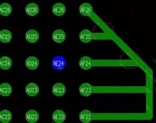
In some high-speed design projects, in order to cope with effect of fiberglass effect on high-speed signals, we can use zigzag wiring technology to slow down effect of fiberglass effect.
Cadence Allegro PCB Editor 16.6-2015 and later supports zigzag layout.
From Cadence Allegro PCB Editor 16.6-2015 menu, select Route -> Unsupported Prototype -> Fiber Weave Effect to open zigzag routing feature.
Time is a deadly knife. Just like 20 years ago, our PCB layout didn't have to pay attention to whether to follow arc line, or worry about effect of PCB plate's fiberglass on high-strength surfaces. speed signal. Maybe in twenty years, when you read this article again, you will feel that old Wu's views are completely wrong...
Therefore, there are no immutable PCB layout rulesexists. With improvement of PCB manufacturing process and increase in data transfer rates, it is possible that current correct rules will become inapplicable in future. Therefore, in order to be a qualified strainer, one must keep up with times and master development of industrial technologies so as not to be thrown out by big waves.
Related
- Can a PCB trace angle be 90 degrees?
- Should PCB trace angle be 90°? — Jumping guide to PCB layout pit
- You can't think about it, can you? A small resistor can be great too
- This is a metaphor for EMI/EMS/EMC that can be understood at a glance.
- USB trace layout experience, a painful lesson
- It suddenly dawned on me that a 0 ohm resistor can still be used like this
- Why can't crystal oscillator be placed on edge of the PCB?
- Case analysis! Why can't crystal oscillator be placed on edge of PCB?
- A Few Design Tips PCB Engineers Need to Know
- The SD card is broken, can it be fixed this way?
Hot Posts
 How to distinguish induction from leakage, we will teach you three tricks! Ordinary people can also learn super practical
- What is drowning in gold? Why Shen Jin?
- This is a metaphor for EMI/EMS/EMC that can be understood at a glance.
- How many types of pads have you seen in PCB design?
- Summary of Common PCB Repair Techniques
- What is three anti-paint? How to use it correctly?
- Knowing these rules, you will not get confused looking at circuit diagram.
- How to make anti-interference PCB design?
- Can diodes do this?