Location:Home Page > Archive Archive
The triode is used as a switch. You should know function of these capacitors which are commonly used.
2023-04-29【Archive】
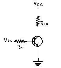
01 Switching transistor circuit diagram
The load resistance is connected directly between triode collector and power supply, and is located in main current circuit of triode. The input voltage Vin controls opening (opening) and closing (closing) of triode switch. When triode, when it is in open state, load current is blocked , otherwise, when triode is in closed state, current can flow. In particular, when Vin is low, because there is no current in base, there is no current in collector, so load connected to collector has no current, which is equivalent to opening switch. At this time, triode operates in cutoff region. Similarly, when Vin is high, base current draws more boosted current through collector, so load circuit is turned on, which is equivalent to closing switch. time triode operates in saturation zone.
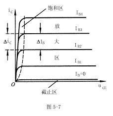
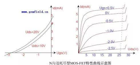
Regarding switching saturation region of transistor, saturation region of MOSFET is gain region of transistor.
The gain of crystal triode is gain of current dependence, i.e. Ic=B*Ib
The magnification of MOS tube is Ic=B*Ugs, which is related to voltage at both ends of g and s. The magnification of MOS tube is relatively large and stable.
02 Select base resistor
(1) First evaluate operating state of triode, whether it is gain region (driving current increase) or saturation region (switching action)
(2) If you are working in gain region, calculate collector current according to collector load parameters, then calculate base current according to gain characteristics of triode, and then calculate resistance according to current value.
(3) If you are working in saturation region, take an NPN lamp as an example to roughly calculate selection value of a typical 3-element switching circuit:
Assuming transistor DC gain is 100, Ib=(drive voltage-0.7Vbe junction voltage drop)/Rb, Vce=Vcc-100Ib×Rc and Vce=0, critical value (saturation region and Increased area critical value) if Rb is less than critical value, but its minimum value is limited by device tolerance Ib and must not be exceeded.
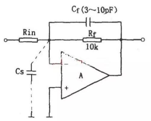
03 Compensation capacitor circuit
The input parasitic capacitance Cs of an amplifier that is normally linear (that is, an amplifier circuit that introduces negative feedback) will affect stability of circuit. Compensation measures are shown in figure. Usually there is a parasitic capacitance Cs on input of amplifier on order of several picofarads, and upper frequency of its bandwidth is about:
ωh=1/(2πRfCs)
To keep gain of amplifier circuit high, more common method is to connect a compensation capacitor Cf to Rf in parallel so that RinCf circuit and RfCs circuit form phase compensation. RinCf will cause phase advance of output voltage. Since value of Cs cannot be known exactly, phase advance and lag cannot be fully compensated. Typically, a variable capacitor Cf is used to minimize extra phase shift by experimenting and adjusting Cf. If Rf=10kΩ, the typical value of Cf is 3~10pF. For a voltage follower, its Cf value may be slightly higher.
04 Op-amp supply bypass capacitor
The bypass is designed to filter out high frequency noise or signals from front stage or power supply. The decoupling ensures a stable output signal of output terminal. The power wire of each built-in op-amp usually needs to take measures to bypass decoupling. ., as shown in figure, as high-frequency bypass capacitor in figure, a ceramic capacitor with excellent high-frequency performance can usually be selected, and its value is about 0.1uF. Or use a 1uF tantalum capacitor. The internal inductance values of these capacitors are all small. In a high-speed op-amp application, bypass capacitors C1 and C2 should be connected to power pin of built-in op-amp, and pins should be as short as possible to form a low inductance ground loop.
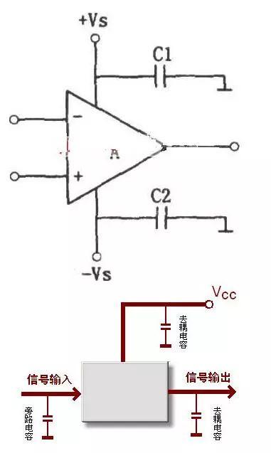
Note. When gain-bandwidth product of amplifier in use exceeds 10 MHz, more stringent measures should be taken to bypass high frequencies. In this case, RF bypass capacitors should be selected. The requirement is small, but not to be ignored. It is usually best to add a set of shunt capacitors every 4-5 devices. Regardless of number of integrated circuits used, at least one set of decoupling capacitors must be added to each PCB.
In a DC power circuit, a change in load will cause power supply noise. For example, in a digital circuit, when circuit switches from one state to another, a large peak current will be generated in power line, forming a transient noise voltage. The configuration of decoupling capacitors can suppress noise generated by load changes. This is a common practice in PCB reliability design. The principles of setting are as follows:
●Connect an electrolytic capacitor with a capacity of 10 to 100 uF to power input terminal. If layout of circuit board allows, using an electrolytic capacitor with a capacity of more than 100 uF will have a better anti-interference effect.
● Set up a 0.01uF ceramic capacitor for each IC chip. If PCB space is too small, you can install a tantalum electrolytic capacitor with a capacity of 1-10uF for every 4-10 chips, and leakage current is very small (less than 0.5uA).
●For devices with weak noise immunity and large current changes at shutdown, as well as storage devices such as ROM and RAM, a decoupling capacitor should be connected directly between power line (Vcc) and ground line (GND) of chip. .
●The leads of decoupling capacitors should not be too long, especially high-frequency bypass capacitors should not be leaded.
In a DC power circuit, a change in load will cause power supply noise. For example, in a digital circuit, when circuit switches from one state to another, a large peak current will be generated in power line, forming a transient noise voltage. The configuration of decoupling capacitors can suppress noise generated by load changes. This is a common practice in PCB reliability design. The principles of setting are as follows:
●Connect an electrolytic capacitor with a capacity of 10 to 100 uF to power input terminal. If layout of circuit board allows, using an electrolytic capacitor with a capacity of more than 100 uF will have a better anti-interference effect.
● Set up a 0.01uF ceramic capacitor for each IC chip. If PCB space is too small, you can install a tantalum electrolytic capacitor with a capacity of 1-10uF for every 4-10 chips, and leakage current is very small (less than 0.5uA).
●For devices with weak noise immunity and large current changes at shutdown, as well as storage devices such as ROM and RAM, a decoupling capacitor should be connected directly between power line (Vcc) and ground line (GND) of chip. .
The leads of decoupling capacitors should not be too long, especially high frequency bypass capacitors should not have leads. In a DC power circuit, load changes can cause noise in power supply. For example, in a digital circuit, when circuit switches from one state to another, a large peak current will be generated in power line, forming a transient noise voltage. The configuration of decoupling capacitors can suppress noise generated by load changes. This is a common practice in PCB reliability design. The principles of setting are as follows:
●Connect an electrolytic capacitor with a capacity of 10 to 100 uF to power input terminal. If layout of circuit board allows, using an electrolytic capacitor with a capacity of more than 100 uF will have a better anti-interference effect.
● Set up a 0.01uF ceramic capacitor for each IC chip. If PCB space is too small, you can install a tantalum electrolytic capacitor with a capacity of 1-10uF for every 4-10 chips, and leakage current is very small (less than 0.5uA).
●For devices with weak noise immunity and large current changes at shutdown, as well as storage devices such as ROM and RAM, a decoupling capacitor should be connected directly between power line (Vcc) and ground line (GND) of chip. .
●The leads of decoupling capacitors should not be too long, especially high-frequency bypass capacitors should not be leaded.
Related
- The triode is used as a switch. You should know function of these capacitors which are commonly used.
- A list of some of the tools commonly used by electronic engineers.
- Anti-reverse connection is very important, make good use of these 4 commonly used circuits
- Count 8 most commonly used diodes! How much do you know?
- Commonly used models of rectifier diodes, what are important parameters?
- A detailed explanation of three commonly used LED drive power schemes.
- 13 Commonly Used Basic Schema Formulas Beginners Should Read
- Countdown of 8 most commonly used diodes
- List of commonly used circuits for zener diodes
- How many of these free and easy to use circuit design programs have you used?
Hot Posts
 How to distinguish induction from leakage, we will teach you three tricks! Ordinary people can also learn super practical
- What is drowning in gold? Why Shen Jin?
- This is a metaphor for EMI/EMS/EMC that can be understood at a glance.
- How many types of pads have you seen in PCB design?
- Summary of Common PCB Repair Techniques
- What is three anti-paint? How to use it correctly?
- Knowing these rules, you will not get confused looking at circuit diagram.
- How to make anti-interference PCB design?
- Can diodes do this?