Location:Home Page > Archive Archive
MOS Lamp Drive Circuit Design Details Engineers Should Know
2023-10-02【Archive】
It is generally accepted that MOSFETs are voltage controlled and do not require any drive current. However, there is junction capacitance between G and S stages of MOSFET, and this capacitance will make driving MOSFET not so easy.
Apart from requirements such as ripple and EMI, faster switching speed of a MOS lamp, better, because shorter switching time, lower switching loss, and switching loss accounts for a large proportion of total loss in switching power supply, so quality of MOS tube drive circuit directly determines efficiency of power supply.
For a MOS lamp: if time required for voltage to change between GS from 0 to lamp turn-on voltage is shorter, faster MOS lamp will turn on. Similarly, if time of voltage drop GS of MOSFET from turn-on voltage to 0 V is shorter, faster MOSFET will turn off.
From this we can learn that if we want to increase or decrease GS voltage in a shorter time, we need to apply more instantaneous drive current to gate of MOSFET.
The commonly used PWM chip output directly drives MOSFET or is amplified by a triode and then drives MOSFET. In fact, instantaneous excitation current has a big drawback.
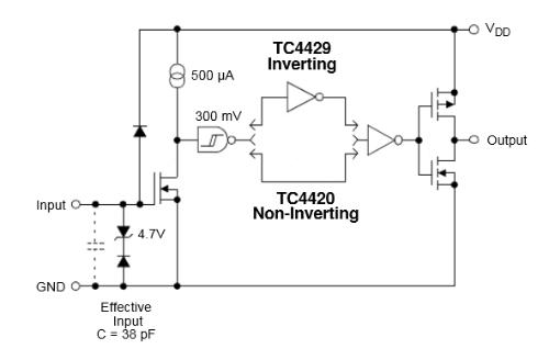
The best method is to use a custom MOSFET driver IC like TC4420 to drive MOS lamp. This type of chip usually has a large instantaneous output current and is also compatible with TTL input level. The internal structure of MOSFET driver chip is as follows:
Attention when designing MOSFET driving circuits:
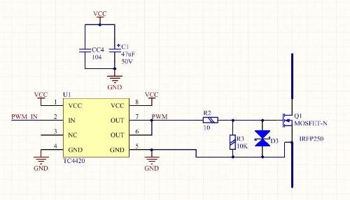
Because there will be parasitic inductance in control circuit wiring, and parasitic inductance and junction capacitance of MOSFET form an LC oscillation circuit. If output pin of driver IC is directly connected to gate of MOSFET, PWM waveform will rise. The falling edge will generate large oscillations, causing MOS tube to heat up or even explode. A common solution is to put a resistor of about 10 ohms in series with gate to reduce Q value of LC tank so that oscillation decays quickly.
Due to high input impedance of MOSFET gate, a little static electricity or interference may cause MOSFET to conduct improperly, so it is recommended to connect a 10kΩ resistor in parallel between MOSFETs G and S. to reduce input resistance.
If you are concerned that interference on a nearby power line will cause an instantaneous high-voltage breakdown of MOSFET, you can connect a TVS transient suppression diode of about 18V in parallel between GS.
TVS can be thought of as a high response voltage regulator tube that can handle hundreds of kilowatts of power instantaneously and can be used to absorb instantaneous interference pulses.
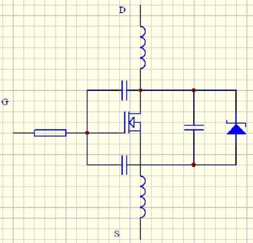
Link to MOS lamp drive diagram:
MOSFET drive circuit wiring diagram:
The circuit area of the MOS lamp driving circuit should be as small as possible, otherwise external electromagnetic interference may be introduced.
The bypass capacitor of driver chip must be as close as possible to VCC and GND pins of driver chip, otherwise wiring inductance will greatly affect instantaneous output current of chip.
General drive waveform of a MOS lamp
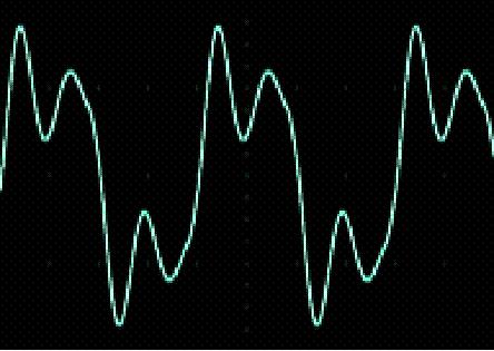
If there is such a round waveform, just wait for a nuclear explosion. Most of time lamps operate in linear region and losses are extremely high.
In general, this situation is such that wiring is too long and inductance is too large, and grid resistance does not help, so you can only redraw the board.
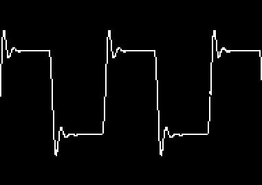
Very disfiguring square wave with high frequency ringing.
The vibration is strong on rising and falling edges, in this case tube usually goes out instantly, which is similar to previous case and goes into a linear region.
The reason is similar, mainly a wiring problem. Thick and round thick pork waves.
The rising and falling edges are very slow due to impedance mismatch.
The control capability of IC is too low or gate resistance is too high.
Resolutely change high current driver chip, and adjust gate resistance to a small adjustment.
The swollen face is filled with a sine triangular wave, born in square wave family.
The resistance of drive circuit is too high. This is obligatory wave of Guangzi. The solution is same as above.
Popular face shape, square wave that everyone loves.
The top and bottom levels are different, and level can currently be called a level because it is flat. The edge is steep, switching speed is fast, loss is very small, and small fluctuations are acceptable. The tube cannot enter linear region. If you have an obsessive-compulsive disorder, you can increase the mesh resistance accordingly.
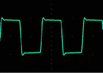
Straight beautiful waves, no ringing, no peaks, no loss of linearity, three-no products, this is most perfect waveform.
Related
- MOS Lamp Drive Circuit Design Details Engineers Should Know
- MOS tube drive circuit, how to make MOS tube turn on and off quickly?
- There are several types of MOS lamp drive circuits, you will understand after reading.
- A Few Design Tips PCB Engineers Need to Know
- The best switching circuit design process for power supplies is a must for engineers!
- Ten Misunderstandings Often Faced by Hardware Engineers When Designing Circuit Stability
- Industrial Computer Circuit Design
- "English abbreviations" that equipment engineers need to know
- Hardware Circuit Design Specification: A Very Good Reference to Hardware Design
- Why are circuit boards mostly green? See what these 20+ engineers have to say
Hot Posts
 How to distinguish induction from leakage, we will teach you three tricks! Ordinary people can also learn super practical
- What is drowning in gold? Why Shen Jin?
- This is a metaphor for EMI/EMS/EMC that can be understood at a glance.
- How many types of pads have you seen in PCB design?
- Summary of Common PCB Repair Techniques
- What is three anti-paint? How to use it correctly?
- Knowing these rules, you will not get confused looking at circuit diagram.
- How to make anti-interference PCB design?
- Can diodes do this?