Location:Home Page > Archive Archive
A Few Design Tips PCB Engineers Need to Know
2023-03-22【Archive】
Introduction
When starting a new project, since most of time is spent on circuit design and component selection, layout and PCB routing, this is often due to lack of experience and insufficient attention.
Failure to devote sufficient time and effort to design during PCB layout phase can lead to problems during production phase or functional defects when design is converted from digital realm to physical realm.
What does it take to create a realistic and reliable board on paper and in physical form? Let's take a look at top 6 PCB design guidelines you need to know when designing a processable and functionally reliable PCB.
1. Fine-tuning component layout
The component placement phase of PCB layout process is both a science and an art, requiring a strategic consideration of major components present on board. While this process can be complex, how you place your electronic components will determine how easy your board will be to build and how well it will match your initial design requirements.
While there is a general general order of component placement, such as sequential placement of connectors, PCB mount components, power circuits, precision circuits, critical circuits, etc., there are some specific guidelines to keep in mind. including:
Orientation. Ensuring that similar components are oriented in same direction will facilitate an efficient and error-free soldering process.
Placement. Avoid placing smaller components behind larger ones as they can be affected by soldering of larger components and cause placement problems.
Organization. It is recommended to place all surface mount (SMT) components on one side of board and all through-hole mount (TH) components on top of board to minimize assembly steps.
A final PCB design note: When using mixed technology components (both through-hole and surface mount), manufacturer may require additional processes to assemble board, adding to overall cost.
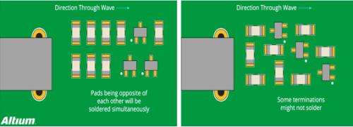
Proper orientation of chip components (left) and incorrect orientation of chip components (right)
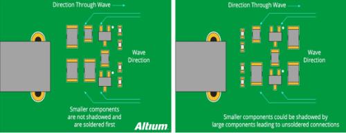
Good component placement (left) and poor component placement (right)
2. Proper placement of electrical wiring, grounding and signal wiring
Once components are placed, power, ground, and signal traces can be placed side by side to provide a clean and uninterrupted signal path. Here are a few guidelines to keep in mind at this stage of layout process:
1) Find power and ground layers
It is always recommended to place power and ground layers inside board, keeping them symmetrical and centered. This helps prevent warping of board, which is also a matter of proper component positioning.
To power IC, it is recommended to use a common path for each power supply, ensure a solid and stable trace width, and avoid connecting power connections in series between components.
2) Signal line connection
Next, connect signal lines according to design in circuit diagram. It is recommended to always use shortest possible paths and direct routing between components.
If your components must be mounted horizontally without deflection, it is recommended that components on PCB be positioned mostly horizontally, and then vertically after components are routed.
This way, as solder migrates during soldering, components will be fixed in horizontal direction. This is shown in top half of figure below. The signal routing method shown at bottom of figure below can cause component deflection due to solder spreading during soldering.
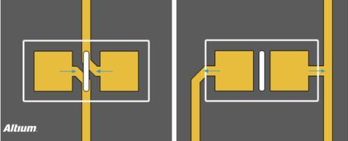
Suggested trace (arrows indicate direction of solder flow)
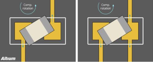
No spacer recommended (arrows indicate direction of solder flow)
3) Determine network width
Your project may require different nets that will carry different currents which will determine required net width. Given this basic requirement, 0.010 in. (10 mils) is recommended for low current analog and digital signals. It should be expanded when your line draws more than 0.3 amps. Here is a free line width calculator that simplifies this conversion process.
3. Effective isolation
You may have experienced how large voltage and current surges in power circuits can interfere with low-voltage current control circuits. To minimize such interference problems, follow these guidelines:
Insulation. Ensures that each power supply shares power and control ground. If you need to wire them together on a PCB, make sure it is as close to end of power path as possible.
Scheme. If you have placed ground plane on an intermediate layer, be sure to place a low impedance path to reduce risk of interference from any power circuits and help protect your control signals. The same guidelines can be followed to separate digital and analog devices.
Communication. To reduce capacitive coupling due to placing a large ground plane and traces above and below it, try to only cross analog ground with analog signal lines.
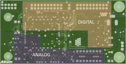
Example of component isolation (digital and analog)
4. Solve problem of overheating
Have you ever had an overheating problem that slowed down performance of a circuit or even damaged PCB? A lot of problems haunted many developers due to fact that they did not take into account heat dissipation. Here are a few guidelines to keep in mind to resolve temperature issues:
1), identify problem components
The first step is to think about which components will remove most heat from board. This can be achieved by first looking up "thermal resistance" rating in datasheet of component, and then following recommended guidelines for transferring generated heat. Of course, heatsinks and cooling fans can be added to keep components cool, and remember to keep critical components away from any high heat sources.
2), add hot air pad
The addition of hot air pads is very useful for production-ready boards and is critical for wave soldering on high copper components and multilayer boards. Due to difficulty of maintaining operating temperature, it is always recommended to use hot air pads for through-hole components to make soldering process as easy as possible by slowing down rate of heat dissipation at component's leads.
In general, always use a hot air pad for any vias or vias that connect to ground or power planes. In addition to hot air pads, you can add drops where pads connect to wires to provide additional copper/metal support. This will help reduce mechanical and thermal stress.
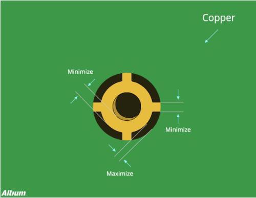
Typical heating element connection
5. Hot air sci-fi pad
In many factories, engineers in charge of process (process) or SMT technology often encounter PCB components with blank solder, wetted or cold solder, etc. A serious problem of lack of wetting, regardless of process conditions are changed or temperature is adjusted reflow oven, there is a certain non-wetting factor. what it is?
Not to mention issue of component and PCB oxidation, after looking into root cause, it was found that most of this type of solder failure is actually due to lack of PCB layout, with most common one being in a specific part of component. Several solder pins are connected to a large area of the copper shell, resulting in poor soldering of these component solder pins after reflow soldering. Some hand-soldered components may also cause incorrect soldering or cladding due to such situations, and some may even be caused by overheating. .Over time, components will be damaged by soldering.
A common PCB often requires a large area to be covered with copper foil for power (Vcc, Vdd or Vss) and ground (GND, Ground) during circuit design. This large area copper foil is usually directly connected to pins of some control circuits (ICs) and electronic components.
Unfortunately, if we want to heat these large area copper foils to melting temperature of tin, it usually takes longer than independent solder pads (i.e. heating will be slower), and heat dissipation is also slower, faster. When one end of such large area copper foil wiring is connected to small components such as small resistors and small capacitors, while other end is not, it is easy to cause soldering problems due to inconsistent melting and solidification time; if adjustment is not good and preheating time is not enough, solder of these components connected with a large piece of copper foil will easily cause virtual soldering problem due to inability to reach melting point.
During Hand Soldering, soldering feet of these components, connected with a large piece of copper foil, will not be able to complete soldering within specified time due to heat dissipation too fast. The most common bad things are cladding and virtual soldering, solder is only soldered to feet of components, not to PCB pads. Judging by appearance, entire brazed seam will form a ball; Moreover, operator constantly increases temperature of soldering iron to solder solder leg to board, or heats it for too long, so that component exceeds heat-resistant temperature and dies damaged without knowing it. As shownbelow.
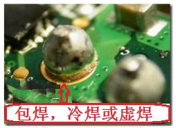
Cold welding, cold welding or virtual welding
Because we know problem, we can find a solution. Generally, we will need a so-called thermal relief pad design (hot air cushion) to solve such a soldering problem caused by a large piece of copper foil connected to solder component. As shown in picture below, wiring on left does not use hot air pads, while wiring on right already uses hot air pad connection method. It can be seen that there are only a few small lines left in contact area between pads and large copper foil. Thus, temperature loss at contact pad can be greatly limited, and a better soldering effect can be achieved.
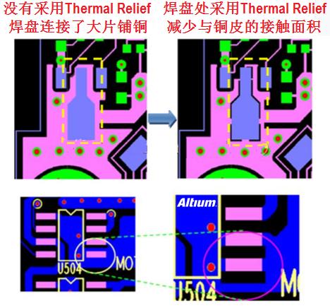
Contrast with Thermal Relief (hot air cushion)
6. Check your work
When you're nonstop humbly assembling all parts for production, it's easy to find problems at end of a design project and get overwhelmed. Thus, double and triple checking your design work at this stage can mean difference between production success or failure.
To facilitate quality control process, we always recommend starting with Electrical Rule Checks (ERC) and Design Rule Checks (DRC) to ensure that your design is fully compliant with all rules and restrictions. With both systems, you can easily check gap widths, line widths, general production settings, high speed requirements and short circuits, and more.
When your ERC and DRC give error-free results, it's a good idea to check routing of each signal, from circuit to board, one signal line at a time, to make sure you haven't missed any information. Also, use probing and masking capabilities of your design tool to make sure your PCB layout materials match your schematic.
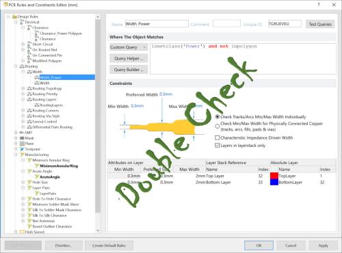
Double check your design, fees, and restrictions
Conclusion
If you have these - Top 5 PCB design tips every PCB designer should know, by following these tips, you will be able to design functional and manufacturable boards in no time, and also have a really high-quality PCB. .
Good PCB design practice is essential to success, and these design rules provide a framework for building and maintaining a practice of continual improvement in all design methods.
Related
- A Few Design Tips PCB Engineers Need to Know
- "English abbreviations" that equipment engineers need to know
- In PCB industry, we all need to know these 5 important common sense rules.
- How to make anti-interference PCB design?
- Do you know layout requirements of some special devices in PCB design?
- (Detailed long text) 7 ways to use diodes that engineers need to master
- The best switching circuit design process for power supplies is a must for engineers!
- What you need to know about semiconductor chips
- About resistors, this is what you need to know
- PCB puzzle, these few special rules!
Hot Posts
 How to distinguish induction from leakage, we will teach you three tricks! Ordinary people can also learn super practical
- What is drowning in gold? Why Shen Jin?
- This is a metaphor for EMI/EMS/EMC that can be understood at a glance.
- How many types of pads have you seen in PCB design?
- Summary of Common PCB Repair Techniques
- What is three anti-paint? How to use it correctly?
- Knowing these rules, you will not get confused looking at circuit diagram.
- How to make anti-interference PCB design?
- Can diodes do this?