Location:Home Page > Archive Archive
The best switching circuit design process for power supplies is a must for engineers!
2023-03-18【Archive】
PCB Fabrication
A very important step in design of any switching power supply is layout of printed circuit board (PCB). If this part is not properly designed, PCB can also make power supply unstable and emit excessive electromagnetic interference (EMI). The role of designer is to ensure that PCB design is reasonable based on an understanding of circuit workflow.
In a switching power supply, some of signals contain rich high-frequency components, so any PCB pin can become an antenna. The length and width of leads affect their resistance and inductance, which in turn affects their frequency response. Even leads carrying DC signals can inject RF (radio frequency) signals from adjacent leads, causing circuit failure or re-radiating interfering signal. All wires carrying AC signals should be as short and wide as possible. This means that any power devices connected to multiple power lines should be placed as close together as possible to keep wire lengths to a minimum. The length of a wire is directly proportional to its inductance and resistance, and width is inversely proportional to its inductance and resistance. The length of wire determines wavelength of its response signal. The longer wire, lower frequency of interference signals it can receive and transmit, and more RF (radio frequency) energy it receives.
Main current circuit
There are four current loops in each switching power supply, and each loop must be separated from other loops. Due to their importance to PCB layout, they are listed below:
1. AC power switch tube loop.
2. AC loop of output rectifier.
3. Power input current loop.
4. Output current load loop.
In fig. 1 a, b and c show outlines of three basic switching power supply topologies.
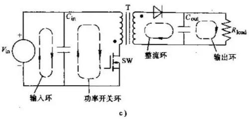
Figure 1 Main current loop in topology of main switching power supply a) non-isolated step-down circuit b) non-isolated step-up circuit c) transformer isolated converter
Normally there is nothing wrong with input power and load current loops. These two loops are mostly DC superimposed with small AC components. As a rule, they have special filters to prevent background noise from entering surrounding circuits. Input and output current loop connections can only be made at terminals of corresponding input and output capacitors. The input circuit charges input capacitor with a near-dc current, but it cannot supply pulsed current required by switching power supply. The input capacitor basically acts as a high frequency energy storage.
Similarly, output filter capacitor stores high-frequency energy in output rectifier, allowing output load circuit to consume DC power. Thus, placement of input and output terminals of filter capacitor is important. If connection between input or output circuit and power switch or rectifier circuit is not connected directly to two ends of capacitor, AC power will flow in and out of input or output filter capacitor and "leave through input and output current circuits . strong>" to external environment.
The AC loop of power switch and rectifier has a very high trapezoidal current waveform typical of a switching PWM power supply. These signals contain harmonics that are well above fundamental switching frequency. The peak value of these AC currents can be 2-5 times continuous input or output DC current. Typical transition times are around 50 ns, so these two circuits are most likely to generate electromagnetic interference (EMI).
In manufacture of power circuit boards, these AC circuits must be wired before other wires. Each circuit consists of three main components: filter capacitors, power switches or rectifiers, inductors or transformers. They are placed as close to each other as possible. These devices are also oriented so that current path between them is as short as possible. On fig. Figure 2 shows a good example of a buck (or buck) converter power section.
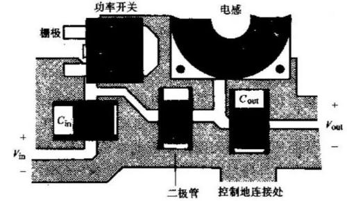
Fig. 2. Perfect Buck circuit diagram
The connection of these current loops also affects measurement of converter efficiency. If voltage drop across these pins is high, converter is less efficient because it operates at a lower voltage (and therefore a higher current). However, if efficiency is measured with a digital voltmeter (DVM) or instrument, measured value at input voltage terminal will be greater than it actually is, resulting in an erroneously large VI product result.
Grounding inside switching power supply
The power ground is a branch of current loop above. As a common potential circuit reference point, power ground plays a very important role in circuit, so placement of power ground must be very careful when laying out PCB. If these bases are reversed, power supply will become unstable.
In addition, one of grounds to consider is ground connecting control IC and its associated passive devices, that is, control ground. This ground is very sensitive and should be placed after all other AC circuits have been installed. The control ground connects to other grounds through some specific points. In general, this connection point is common connection point for all devices that generate a small voltage that control IC needs to detect. It includes common junction of current sense resistor of current source converter and lower end of output resistor divider. The purpose of this is to reduce noise introduced by connection between measurement section and sensitive input of voltage or current error amplifier. If control ground is connected to other places, noise generated by these main circuit circuits will be added to control signal, affecting normal operation of control IC.
See rice. 3, which shows location of ground wire of main conversion topology.
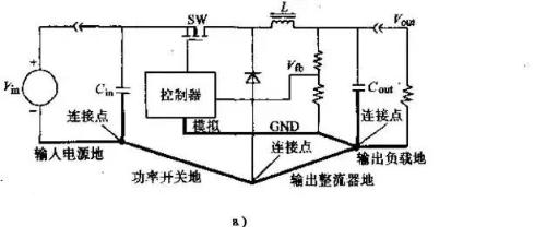
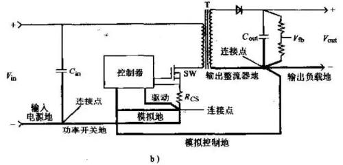
Figure 3. Bottom of main conversion topologies a) DC-DC converter without isolation b) Coupled converter without isolation transformer c) Coupled converter with isolation transformer
Each high-current ground wire should be short and wide. As a general rule, common terminal of input filter capacitor should be only contact for other AC grounds besides control ground.
AC voltage node
Each switching power supply has a node with highest AC voltage, which is drain (or collector) of power switch. In non-isolated DC/DC converters, this node is connected to an inductor and a freewheeling diode. There are as many AC nodes in a transformer isolation topology as there are windings in a transformer. But from an electrical point of view, they are one and same node, but are converted by converter into many nodes. Each communication node must be carefully considered individually.
AC nodes present unique problems because AC voltages can easily capacitively couple to adjacent terminals on different layers, radiating electromagnetic interference. What is more unfavorable is that this part of wire must be used as heat dissipation part of power switch tube and rectifier, especially in surface mount power supplies. From an electrical point of view, these leads should be as narrow as possible, but from a thermal point of view, wider better. In surface mount design, best compromise method is to make top layer of PCB same as the bottom layer and connect them via multiple vias (or through holes) as shown in Figure 4.
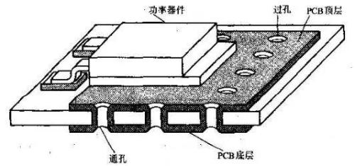
Fig. 4. Improved connection method to improve heat dissipation ability of PCB surface and reduce capacitive coupling with other PCB pins
This approach more than doubles cooling volume and surface area, and greatly reduces capacitive coupling to other pins. When using vias, other signals and ground must be separated from these high voltage leads and their heatsinks. In a stand-alone drive, ground will draw power from these nodes through a heat sink (separated from drain by an insulator) and drain away from product through AC power plug.
Parallel connection of filter capacitors
To reduce equivalent series resistance (ESR) of filter capacitor, several capacitors are often connected in parallel. At same time, it can also divide ripple current into each capacitor, so that each capacitor can work at rated ripple current. To evenly distribute ripple current, make each capacitor same as output impedance of ripple current source. This means that length and width of connection between rectifier or circuit breaker and each capacitor terminal must be same.
In fig. 5a shows a way of arranging capacitors in a row and connecting them in series so that capacitors located near circuit breaker tube or rectifier share a much larger ripple current than capacitors located farther away. service life of capacitors that are located closer to each other. The parallel capacitor connection method shown in fig. 5b is more appropriate.
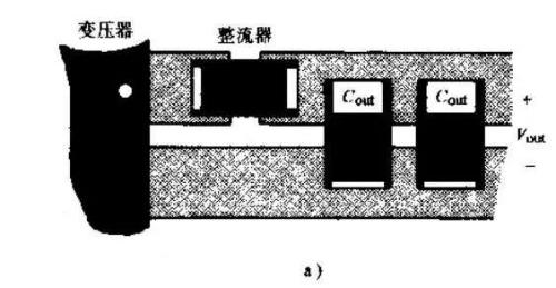
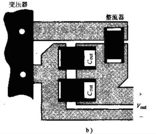
Figure 5. Arrangement of parallel capacitors a) Unreasonable arrangement of parallel capacitors b) Ideal arrangement of parallel capacitors
Designers should do their best to place capacitors on both sides of circuit in a "radially symmetrical arrangement" from ripple current source.
The best way to make a switching power supply PCB
The best way to organize a switching power supply is similar to its electrical circuit. The best design process looks like this:
1. Place transformer or inductor;
2. Organize current loop of power switch tube;
3. Organize current loop of output rectifier;
4. Connect control circuit to AC power circuit;
5. Position input loop and input filter;
6. Install output load circuit and output filter.
A good rule of thumb is to copper PCB as much as possible, that is, make sure that there are no large empty areas on PCB. To fill empty space, ground and power wires can be thickened.
This has two advantages: first, it improves heat dissipation of inverter; secondly, a large area of copper can trap RF energy and dissipate it well through eddy currents.
Of course, power supply is usually located at end, so placement space is very small and location is not ideal, so there is no need to design PCB strictly according to above process. Every designer must understand importance of electrical surface. Based on parts, make your own best design.
Related
- The best switching circuit design process for power supplies is a must for engineers!
- Notes on whole switching power supply design process!
- Analysis of damping RC circuit of a switching power supply "haberdashery"
- Finally, it becomes clear that process of obtaining switching losses of a MOSFET in a switching power supply
- Engineer Daniel tells you: The "Y Capacitor" of a switching power supply is calculated in this way.
- Frequently Asked Questions for USB Interface Circuit Design
- Switching Power Supply PCB Design Skills
- Detailed analysis of the "various protection schemes" of a switching power supply
- Four ways to reduce the output "ripple and noise" of a switching power supply
- Power Knowledge - Flyback Transformer Design Process
Hot Posts
 How to distinguish induction from leakage, we will teach you three tricks! Ordinary people can also learn super practical
- What is drowning in gold? Why Shen Jin?
- This is a metaphor for EMI/EMS/EMC that can be understood at a glance.
- How many types of pads have you seen in PCB design?
- Summary of Common PCB Repair Techniques
- What is three anti-paint? How to use it correctly?
- Knowing these rules, you will not get confused looking at circuit diagram.
- How to make anti-interference PCB design?
- Can diodes do this?