Location:Home Page > Archive Archive
Hardware Circuit Design Specification: A Very Good Reference to Hardware Design
2023-03-18【Archive】
Hardware Circuit Design Process Series - Circuit Design (Category)
1. Hardware Circuit Design Process - Hardware Circuit Design Specification
2. Hardware circuit design process - circuit design (1): main chip selection3. Hardware circuit design process - circuit design (2): chip selection4. Hardware circuit design process - circuit design ( 3): power consumption analysis and power supply design5. Developing a hardware design process diagram (4): designing a suitable system power supply
01
Hardware Schematic Specification
1. Examine design requirements in detail and separate circuit functional modules and performance requirements from requirements;
2. Formulate an overall design plan according to function and performance requirements, and select a CPU.CPU selection has following requirements:
a) High performance;b) Ease of development: this is reflected in many types of debugging hardware, a large number of reference designs, extensive software resources, and many successful cases;c) Good scalability;
3. For selected CPU chip, select a successful reference design that is close to our needs. Typically, CPU manufacturers or their partners do some design work for each CPU chip. For example, 440EP has yosemite development board and bamboo development board. We mean yosemite development board. Although reference design diagram provided by manufacturer to user is not a product-level thing, it should be strictly verified. This will affect popularization and application of their chips . Even if peripheral circuits of reference design are deliberately done, way pins of CPU itself are connected certainly deserves our trust.
Of course, if there are several reference designs with different pin connection methods, you can carefully read CPU chip manual and error details, or find manufacturer to confirm; In addition, before designing, we are best to borrow or buy an option. If there is no problem, then hardware reference design is also reliable, but it should be noted that many processors now have multiple startup modes, we need to choose most appropriate startup mode, or make it a compatible design.
4. Select peripheral function module components according to your requirements. When choosing components, you should be guided by following principles:
a) The principle of universality: selected components should be widely distributed and tested, and cold-biased chips should be used as little as possible to reduce risks;b)High economic principle: with similar function, performance and utilization rate. Under certain circumstances, try to choose components with better prices to reduce costs; c) principle of convenient procurement: try to choose components that are easy to buy and that have a short delivery cycle; d) Sustainable development principle: try to choose components that will not be phased out in foreseeable future;e) Replaceability principle: try to choose pin-compatible components with a large number of types;f ) Upward compatibility principle : try to choose old products that were used before components;g) principle of saving resources: try to use all functions and pins of components;
5. Change peripheral circuit of selected CPU reference design circuit diagram. When changing, it is necessary to find at least 3 successful reference designs of same peripheral chip for each functional module. If connection methods of reference design are found, they are all same, so in principle you can safely refer to design, but even if there is only one a reference project that is different from others, you can't just obey majority. with multiple sides, contact chip factory technical support, and finally determine scientific and correct connection method. If you still have doubts, you can make a compatible design; this is most important part of whole circuit design process. We need to do following:
a) For each functional module, try to find as many successful reference designs as possible. The more complex it must be, more successful reference designs are experience and richness of "predecessors". We should learn from them and stand on "predecessors" "On shoulders", you have improved your starting point;b) You should ask and learn more from authorities, but you should not be superstitious about authorities, because everyone has cognitive errors, and it is difficult to guarantee that even what you know best can always give most scientific understanding and judgment, developers must make most scientific and correct decision based on extensive research, study and discussion;c) If this refers to existing old product design, design We must pay attention to legacy problems of old products. These legacy problems are related to what kind of functional hardware modules. When developing these related modules, we must pay more attention to careful analysis and not copy original design mechanically. For example , IDE in our older products often has problems. After careful consideration, detailed discussion, and with citing other successful designs, we found that our IDE interface has two non-standardized pin connections; in addition, for video sync signal loss problemization in FGPI channel, output of hardware clock signal can be taken out into hardware design for further verification and better disclosure of essence of problem;
6. The design of circuit diagram of equipment must also follow some basic principles that must be implemented throughout design process. Although these principles are also reflected in successful reference design, because we can be a schematic diagram spelled out, so we are all would still have to develop and test our schematic diagram according to these principles at any time, these principles include:
a) Separate digital power and analog power;b) Separate digital ground and analog ground, single point ground, digital ground can be directly connected to chassis ground (ground), and chassis must be connected to ground;c ) Make sure that resources of each module in system do not conflict, for example: addresses of devices on same I2C bus cannot be same, etc.;d) Read manuals of all chips in system (usually these are manuals by design) to see their unused inputs. ;e) Attempt to provide ease of software development without complicating hardware design, or In exchange for more convenient, reliable, and efficient software design with less hardware design complexity, this requires hardware developers to understand development process and debug basic software that requires high requirements;e) power consumption problems;
g) To solve problem of product heat dissipation, heatsinks or fans can be added to chips with large power consumption and heat dissipation. This issue should also be considered in product case. The chassis cannot be turned into a box to keep warm. The circuit board is cold for "greenhouse"; Also consider location of product, it is best to place it in a place with relatively large space and smooth airflow, which is conducive to heat dissipation; /p>
7. After design of equipment circuit diagram is completed, designer must first conduct a self-test according to above steps and requirements. After self-test, he must be more than 95% sure. and trust, strong>Then send it to others for review. Other reviewers will also rigorously review schema according to above requirements. If problems are found, they should be discussed and analyzed in time. The analysis and solution process also follows above principles and steps; 8. As long as development and verification personnel can strictly follow above requirements to circuit design and review, we have reason to believe that probability of success of first version is notThe private circuit board developed by all hardware developers will be very high, so a few points:
a) It is up to designers themselves to ensure correctness and validity of circuit diagrams. Design achievement is a review, rigorous self-examination, do not place your hopes on reviewers, and any problems in design should be resolved by designers themselves Assumes that other auditors are not jointly and severally liable; b) Although other auditors are not jointly and severally liable, they must carry out rigorous audits in accordance with above requirements. it also reflects level, style and attitude of auditors; c) Conventional schematic design, including retrofits and modifications to older products, in principle requires that first version of schematic be successful, and no more than two versions of second. board will be closed and if more than two versions are exceeded there will be performance penalties;
d) For new designs with complex features and many doubts, circuit diagrams are fundamentally needed. If it is successful within two releases, board will be sealed up to three releases, and performance penalties will be imposed if more than three releases are exceeded;e) Standard for principle sealing: have any principal flying leads and other processing points;
9. Specific rewards and penalties related to design of schematic diagrams mentioned above will be formulated after careful investigation and research, and published and implemented after obtaining consent of company's leaders; 10. The purpose and starting point of formulating this "Technical Specification" is to cultivate a strict and pragmatic work style and a serious and serious attitude to work of hardware developers, enhance their sense of responsibility and mission, and improve work efficiency and development success Efficiency, to ensure product quality , I hope young hardware developers can quickly grow in learning! For corresponding analog circuit products we are currently developing, there are no problems with main chip, peripheral chips and inter-chip connections. Therefore, the choice of components is especially important, and some basic principles of hardware design need to be taken into account.
02
Main Chip Selection
The choice of platform is often related to algorithm chosen by system, so if you want to improve architecture and design capabilities of a platform, you must continually improve your own algorithm, complexity estimation capabilities, and throughput analysis capabilities.
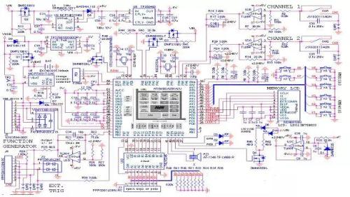
Commonly used main processor chips are: MCU, ASIC, RISC (DEC Alpha, ARC, ARM, MIPS, PowerPC, SPARC and SuperH), DSP and FPGA, etc. There are many articles on Internet comparing these processors, here no cliché, just a typical choice of main processor here. For example, there are many high definition network camera (HD-IPNC) design requirements in market, and IPNC solutions appear in an endless stream: Hi3512, Hi3515, Hi3520, etc., and solutions provided by NXP include PNX1700, PNX1005, etc. For HD-IPNC core processing chip, there are several main technical indicators: video resolution, video encoding algorithm, maximum image capture resolution supported, CMOS image pre-processing capability, and network stack development platform protocols. Single Chip Hi3512 Realizes 720P30 H.264 Encoding and Decoding Capabilities, Corresponding to HD IP Camera Applications Hi3515 can realize 1080P30 encoding and decoding capabilities, continuously improving performance of HD IP Camera. One DM355 chip implements 720P30 MPEG4 codec, one DM365 chip implements 720P30 H.264 codec, one DM368 chip implements 1080P30 H.264 codec.
DM355 was released in third quarter of 2007, DM365 in first quarter of 2009, and DM368 in second quarter of 2010. Almost simultaneously, HiSilicon solutions of same level appeared. HiSilicon and TI solutions are based on Linux. For network protocol stack development, there is no difference in resources of open source community. The only difference is SDK development kit provided by chip vendor. There is a certain distance between them, but development of linux network is not a technical difficulty, therefore does not affect promotion of products. As an IPNC solution, in 720P era, Hisilicon's solution has an advantage over TI's solution in that it supports H.264 codec algorithm, while TI only supports MPEG4 codec algorithm. Although in early 2008 shortcomings of MPEG4 began to be reflected in market, but at that time it did not seem to affect promotion of DM355. For highest image capture resolution supported, HiSilicon's solution can support JPEG capture at 3 megapixels at 5 fps, and DM355 can support up to 5 megapixels, although it has not been successfully designed to capture 5 megapixels (memory) . a bit of a distribution issue, so I won't talk about it later), but at least 4M Pixel capture is implemented, and a few friends have been able to capture 2560x1920, which is close to 5M Pixel, so DM355 wins a bit in this regard. Because in high-definition resolution, CCD sensor is very expensive, and raw size of CMOS sensor is small, resulting in poor image quality of CMOS sensor in low light conditions. worse, so TI has integrated an image pre-processing module called ISP into DM355 processor, which consists of CCDC, IPIPE, IPIPEIF and H3A modules, which can help convert CMOS RAW DATA (usually refers to Bayer format data) to YCbCr data, while realizing white balance adjustment, histogram statistics, auto exposure, auto focus and other functions required by CMOS solutions, so DM355 processor can seamlessly communicate with various image sensors. However, HiSilicon solution has limitations in choosing CMOS and it can only use some OVT solutions because some OVT sensors integrate image pre-processing functions. However, DM355 can connect not only to OVT solutions, but also to many third party CMOS sensors such as Aptina's MT9P031. So in terms of image pre-processing capabilities, DM355 continues to win.
In field of IPNC, as long as each device earns 1 USD, it can start to increase in volume, so in that era, few people paid attention to performance difference between H.264 and MPEG4, and TI provided market Very good waiting, DM365 with H.264 support will be available soon. Therefore, for IPNC solution, many companies at that time chose DM355 solution. Some people I know now have successfully switched from DM355 to DM365 and DM368. Although you sometimes scold TI, why wasn't technology better? Back then it was done in one step, and so much performance wasted. However, technology accumulates bit by bit, and for individuals there is no ambiguity, and for large companies they cannot make a big leap forward. The DM355 CMOS pre-processing technology also has many bugs, and SDK also has many bugs that sometimes make you love and hate, but technology is not always perfect, which is good if it can meet market demand in specific historical conditions. , thing. Of course, HiSilicon's solution also shines in DVS and DVR, which is just as good as TI's solution. To select other chips, you can refer to chip manuals on official websites of each chip manufacturer for comparison.Currently, chip manuals of most chip manufacturers are downloaded without NDA. If there are non-disclosure issues, it depends on ability of user and company to manage resources. Generally, find general agent of relevant chip in China, contact and sign NDA to obtain relevant information. Go to office once every two weekshome pages of major chip manufacturers and pay attention to chip design. This is a must for every electronics engineer. This not only accumulates enough capital to develop next solution, but also contributes to development of company's product. homework strategy.
03
Buying chips
Purchasing chips is an integral part of electronic circuit design process. In general, until chips that can be found from major IC manufacturers are removed by EOL, they can usually be bought. However, as an electronics designer, he seldom faced challenge of purchasing chips. Common situations are:
1. In face of economic crisis, various IC manufacturers have scaled back production, resulting in extended chip delivery cycles, with some IC manufacturers even offering a 20-week order term. I was very impressed when I ordered PTH08T240WAD in first half of 2009 and I received goods within 4-6 weeks, but in second half of 2009 either delivery time was 20 weeks, or price doubled, and there were only a few of them . 2. Although some chips have industrial-grade products in datasheet, but due to very small number used in market, production of IC manufacturers is very small, and market supply is also very scarce, which makes it necessary to do enterprises with high-temperature products of industrial class or military grade products pay a hefty price. 3. Some chip manufacturers control their agent channels very strictly. Some relatively new chips cannot be bought from ordinary traders, so they can only be ordered from agents. If quantity can meet MPQ or MOQ requirements, general agents will help you purchase. But if you just want one or two engineering samples, if you have a product, then it depends on your relationship with agent. If you are new to this industry, then it is very likely that you will not be able to get this engineering sample from agent.
4. The sale of some chips is limited. If chips are only for China and not for Asia, they can usually be obtained through Singapore. If chips are only for Asia, difficulty of acquiring will increase significantly. purchase price will be far beyond your imagination. First, take a look at case of purchasing chip:I recommended FPGA chip to a friend and he sent me a chat recording as follows:
2010-8-3 9:13:12 A B XC6SLX16-2CSG225C Order 250.002010-8-3 9:22:10 B A How long does it take to order? 2010-8-3 9:22:37 A B 2 weeks2010-8-13 14:22:47 A B XC6SLX16-2CSG225C You ordered this model from me on same day, delivery time is two weeks, but this model is a sensitive model. It is embargoed in China. We need a third party to buy it, so time tothe stay is about 5 weeks. Do you think this is acceptable?
Note. B is buyer of chip, A is supplier of chip.Look what happened at time:August 3, 2010, design B A. Good plan, after confirming chip model, because chip model is relatively new, I was afraid that chip would be out of stock, so I confirmed chip source with chip supplier A. After knowing price and delivery date, B was very pleased and very satisfied. Tell me if chip you recommend is really cost effective and I will place an order as soon as schematic design is complete.
August 13, 2010, after B finished designing circuit diagram, when B wanted to place an order with A, he unexpectedly received above response from A, so he was immediately confused because PCB layout may be completed in 2 weeks, 1 week can complete PCB processing production. This means that even if B had placed order on August 13, 2010, he would have to wait 2 weeks before starting welding and debugging. (Eventually supplier A found out that chip was banned from China and it was impossible to help B get it. It ended up taking 5 weeks for C to buy it from another chip dealer and price went up to 450)A delay of 2 weeks can be considered a small amount. Under other special circumstances, it is possible that chip cannot be received. Crying, if you encounter such a situation after PCB layout is ready, you will cry without tears. Therefore, it is recommended to place an order for purchase of chips immediately after confirming decision on chip. Sometimes price and shipping information received at time of chip request may be inaccurate,because IC industry database Updates sometimes have a certain lag, and dust will settle only after order is placed and contract with supplier is confirmed.
04
Energy analysis and power supply design
Analysis of ripple requirements of main system chip
Because a regulated DC source is usually formed by rectifying and stabilizing an AC source, it is inevitable that there will be some AC components in regulated DC amount. This AC component is superimposed on regulated DC amount and is called ripple. The ripple has many negative effects on system, for example, if ripple is too high, it will cause main processor chip to restart or introduce noise into some ADs and DAs.
It is a common occurrence that if ripple of power supply is superimposed on output of DA audio chip, it will cause a buzz. The following table shows ripple requirements of chip used in project and ripple range that can be provided.Read the power chip. Ripple is an important parameter when choosing a power supply chip. Only one or two chips are shown for illustration purposes: Chip ripple statistics:
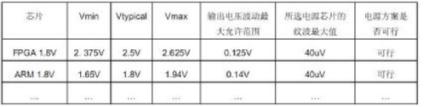
Analysis of series voltage requirements of main system chipMost modern electronic products require use of several supply voltages. Increasing number of supply voltages is a challenging design challenge when it is necessary to control relative turn-on and turn-off characteristics of power supplies to ensure that digital system is not damaged or latched. Typically, this will be detailed in IC manual, and it is recommended that you follow requirements of IC manual when designing. Analyzing power consumption of all microcircuits in system
In order to calculate power consumption of all chips used on board, power consumption of most chips is detailed in chip manual, and power consumption of some chips is not clearly stated in manual, such as FPGA, on page this time, you can according to experience of previous development or write FPGA logic in advance, use EDA tools for statistics, such as Xpower Analyzer ISE, following table is a statistical case of power analysis.
Note. Since there is a lot of data, only a few 3.3 V chips are selected for statistics.
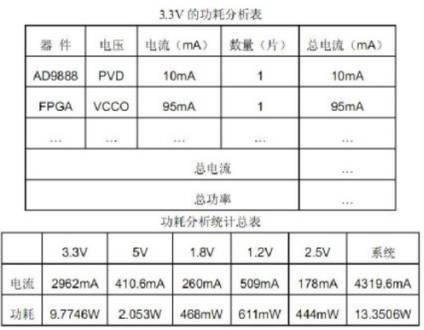
Demonstrate whether selected power solution meets all of above requirementsAccording to requirements of power-up sequence, ripple analysis and power consumption, select right power solution . Designing a power supply is a delicate job, and statistics and data sorting are a must. Developing good design habits is a necessary link for "talking on same board." There is a lot of knowledge about choosing power solutions and there are countless articles on analysis. Here are just some of patterns. In consumer products, because cost is very sensitive and heat dissipation requirements are relatively high, they generally prefer DC/DC solutions, and now more and more tend to multi-channel power management ICs (PMIC) . solution. A relatively big disadvantage of DC/DC is large ripple, besides, if design of inductor and capacitor is unreasonable, voltage will be very unstable.
I was very impressed that after DC/DC was used to power FPGA, according to analysis of FPGA Power Distribution System (PDS), enough 330uF tantalum capacitors were added. As a result, DC/DC often had problems, so DC/DC DC must be carefully designed. When designing high-power circuits, choice of inductor is also very important. Many inductor models in reference design are not available in Beijing Zhongfa Electronics Market or Shenzhen SEG Plaza, and saturation current of domestic market substitutes is often higher. This is less than required inductance value in reference design, so it is recommended to purchase an inductor that meets requirements before proceeding with manufacture of inductor footprint. In field of non-consumer products, LDOs and power modules are used relatively more because power supply ripple is small and design is simple. When I first started learning circuits, I was very concerned with DC/DC design, so at that time I used LDOs and power modules until I started designing consumer products, due to cost considerations, I had to start DC/DC design. , but now chip manufacturers have mostly integrated MOSFETs into chip, so DC/DC design complexity has also become less.
05
Design a suitable system power supply
For a modern electronic system, design of power supply is becoming more and more important. I would like to discuss with you some of my own experience in power supply design so that we can better understand what a power supply is. design and progress. Q1: How to estimate power requirements of a systemAnswer: A real electronic system needs carefulbut analyze its nutritional requirements. Not only take care of input voltage, output voltage and current, but also carefully consider total power consumption, power supply efficiency, power supply part transient load variation, tolerance range of key components. to fluctuations in power supply and corresponding allowable power ripple, heat dissipation and so on. Power consumption and efficiency are closely related. If efficiency is high, total power consumption will be less when load power consumption is same, which is very beneficial for power budget of whole system. Compared with LDO and switching power supply, efficiency of switching power supply is higher. In this case, efficiency rating is based not only on efficiency of power supply circuit at full load, but also on level of efficiency at low load. Regarding transient load response capability, there will be strict requirements for some high-performance applications of CPU, because when CPU suddenly starts to perform heavy tasks, required starting current is very large if power supply circuit response speed is insufficient, which results in too much and too little instantaneous voltage drop, causing CPU to misbehave. Generally speaking, actual value of required power is basically +-5% of rated value, so allowable power ripple can be calculated based on this, and a margin must of course be reserved. Heat dissipation is more important for high current power supplies and LDOs, and it can also be assessed if it is suitable for calculations. Question 2. How to choose a suitable power supply circuit
Answer: According to specific technical data obtained from analysis of system requirements, you can choose appropriate power supply to implement circuit. Generally, for low-current part, it includes an LDO (linear power converter), a switching power supply capacitor buck converter, and a switching power supply inductance capacitor converter. On contrary, LDO design is easiest to implement and output ripple is small, but disadvantages are that efficiency may not be high, heat dissipation may be large, and current that can be provided is small compared to switching power supply. The switching power supply circuit has a flexible design and high efficiency, but ripple is large, implementation is more complicated, debugging is more cumbersome, and so on. Q3: How to choose suitable components and parameters for switching power supply circuitAnswer: Many engineers who have not used switching power supply design will have a certain feeling about about it. For example, worry about switching power supply noise, PCB layout, choice ofmeters and component types, etc. In fact, if you understand this, it is very convenient to use a switching power supply design. The switching power supply usually includes a switching power supply controller and an output. Some controllers will integrate MOSFETs into chip, which is easier to use and simplifies PCB design, but design is flexible. Sex is reduced. The switching controller is basically a closed-loop control system, so generally there will be a sampling circuit for feedback output voltage and a control circuit for feedback loop. Thus, design of this part is to provide an accurate sampling scheme and feedback depth control, because if feedback loop response is too slow, step response will be greatly affected. The design of output part includes output capacitors, output inductors, MOSFETs, etc. Their choice is mainly determined by balance between performance and cost. For example, if switching frequency is high, a small inductor can be used. value (means small package and cheap cost), but high switching frequency will increase noise and switching loss of MOSFET, which will reduce efficiency. The result of using a low switching frequency is opposite.
The ESR of output capacitor and choice of Rds_on MOSFET is also very critical. A small ESR can reduce output ripple, but cost of capacitor will increase and a good capacitor will be expensive. Also pay attention to controllability of switching power supply controller, too many MOSFETs are poorly controlled. Generally speaking, switching power controller vendors provide engineers with specific calculation formulas and usage patterns. Q4: How to debug switching power supply circuitAnswer: I have some experience that I can share with you1: The output of power circuit is connected through a large resistor power with low resistance to board, so that power circuit can be debugged first without soldering resistor, and influence of subsequent circuit can be avoided. 2: Generally speaking, switching controller is a closed-loop system. If output degradation exceeds closed-loop controlled range, switching power supply will not work properly, so in this case, you must carefully check feedback and sampling circuit. Especially if an output capacitor with a high ESR value is used, a lot of power supply ripple will be generated, which will also affect operation of switching power supply. Discussion of grounding technologyQuestion 1: Why is grounding necessary?Answer: Initially, technologistsi grounding was designed to prevent damage to electrical or electronic equipment. The purpose of protective measures taken by lightning is to inject lightning current generated by lightning into ground through a lightning rod in order to protect building. At same time, grounding is also necessary to protect people
An effective means of personal safety. When a phase line (such as poor wire insulation, aging lines, etc.) touches equipment case for any reason, dangerous voltage will be generated on equipment case. , and resulting short circuit current will flow through PE line to ground, thus playing a protective role. With development of electronic communications and other digital fields, it is far from sufficient to consider only lightning protection and safety in earthing system. For example, in a communication system, interconnection of signals between a large number of devices requires each device to have a reference "ground". As a reference ground for signals. In addition, with complexity of electronic equipment, frequency of signal becomes higher and higher, so when designing grounding, special attention must be paid to electromagnetic compatibility issues such as mutual interference between signals, otherwise improper grounding will seriously affect reliability. work system sex and stability. Recently, concept of "ground" has also been introduced into high-speed signal return technology. Q2: Definition of groundingAnswer: In modern concept of grounding for line engineers, this term usually means "line voltage reference point". ; for system designers, this is often a cabinet or rack; for electrical engineers, this means green protective earth or ground connectionmeaning. A more general definition is that "ground is a low impedance path through which current returns to its source". Note that requirements are "low impedance" and "access". Q3: General ground symbolsAnswer: PE, PGND, FG - protective earth or chassis, BGND or DC-RETURN - DC - 48 V (+ 24 C) return of power source (battery); GND - working ground; DGND - digital ground; AGND - analog ground; LGND - Lightning Protection GroundingQ4: Proper grounding methodAnswer: There are many grounding methods, including single-point grounding, multi-point grounding, and mixed types of grounding. Single-point grounding is divided into serial single-point grounding and parallel single-point grounding. Generally speaking, single-point grounding is used for simple circuits, grounding differences between different functional modules, and low-frequency (10MHz frequency) circuits require multi-point grounding or multi-layer boards (full ground layers).
Q5: Introduction to signal backflow and cross-segmentationAnswer: An electronic signal needs to find lowest impedance path to return current to ground, so how to deal with this signal return becomes very important. Firstly, from formula you can find out that radiation intensity is proportional to area of the loop, that is, longer return path must be, larger resulting ring and more interference to external radiation. Therefore, PCB layout When designing a board, power loop area and signal loop should be reduced as much as possible. Secondly, for a high-speed signal, ensuring a good signal return can guarantee quality of its signal, since characteristic impedance of a transmission line on a printed circuit board usually refers to ground plane (or power plane). If there is a continuous ground plate near high speed line, impedance of this line can remain continuous. If there is no ground near segment line, impedance will change and discontinuous impedance will affect signal. . Therefore, when wiring, high-speed line should be located on a layer close to ground layer, or one or two ground lines should be laid in parallel next to high-speed line to perform function of shielding and protection. providing a return nearby. Third, why try not to separate power supply when wiring, this is also because after signal crosses different power levels, its return path will be very long and it will be easily disturbed. Of course, it is not strictly required that power not be shared, and this is possible for low speed signals because noise generated can be neglected compared to signal. For high-speed signals, you must carefully check and try not to cross them. You can adjust power wiring. (For multiple power supplies on multilayer boards)
Question 6. Why and how to separate analog and digital ground?Answer: Analog and digital signals must return to ground because digital signals change rapidly, so noise, caused by digital ground will be very large, and a clean ground is required for analog signal to work. If analog and digital bases are mixed, noise can affect analog signal. Generally speaking, analog ground and digital ground must be processed separately and then connected together in thin traces or connected together at same point. The general idea is to try and block output of noise from digital ground to analog ground. Of course, it's not a very hard requirement that analog ground and digital ground should be separated. If digital ground next to analog part is still very clean, they can be connected together. Q7: How to ground signals on one board?Answer: For general purpose devices, it is best to use nearest groundwiring using a full ground plate After multilayer board is designed, it is very easy to ground common signal. The basic principle is to ensure wiring continuity and reduce number of vias; close to ground plane or power plane, etc. Q8: How to ground interface devices of board?Answer: Some boards have external input and output interfaces, such as serial port connectors, network port RJ45 connectors, etc., if their grounding design is not good, it will also affect normal operation, such as network port connection has error codes, packet loss, etc., and this will become a source of electromagnetic interference from outside, and noise inside board will be transmitted to outside. Generally speaking, independent interface ground is separated separately, and signal ground connection is connected with a thin wire, and a 0 ohm or low resistance resistor can be connected in series. Thin traces can be used to block interference from signal ground to interface ground. Similarly, filtering of interface ground and interface power should be carefully considered.
Q9: How to ground shield layer of cable using shield layer?Answer: The shield layer of shielded cable must be connected to ground of board interface. instead of signal ground, this is because there are various noises on signal ground, if shield layer is connected to signal ground, noise voltage will induce a common mode current that will interfere outward along shield layer, so poorly designed cables tend to be most large noise source of electromagnetic interference. Of course, interface ground is also assumed to be very clean.
Related
- Hardware Circuit Design Specification: A Very Good Reference to Hardware Design
- Commonly Used Peripheral Diagrams, Hardware Design Reference and Precautions
- 50 Common Hardware Design Patterns
- How to design a triode amplifier circuit
- Hardware Collection: 50 Common Circuit Diagrams
- Industrial Computer Circuit Design
- Ten Misunderstandings Often Faced by Hardware Engineers When Designing Circuit Stability
- The best switching circuit design process for power supplies is a must for engineers!
- How many of these free and easy to use circuit design programs have you used?
- A Few Design Tips PCB Engineers Need to Know
Hot Posts
 How to distinguish induction from leakage, we will teach you three tricks! Ordinary people can also learn super practical
- What is drowning in gold? Why Shen Jin?
- This is a metaphor for EMI/EMS/EMC that can be understood at a glance.
- How many types of pads have you seen in PCB design?
- Summary of Common PCB Repair Techniques
- What is three anti-paint? How to use it correctly?
- Knowing these rules, you will not get confused looking at circuit diagram.
- How to make anti-interference PCB design?
- Can diodes do this?