Location:Home Page > Archive Archive
(Detailed long article) Detailed interpretation of twelve modes of operation of a phase-shifted full bridge.
2023-11-22【Archive】
In early days of large power supplies (over 1kW output), most widely used topology was Full-Bridge hard switching topology, which has a fixed switching frequency and voltage and current that patch tube can handle. Small loads, easy to control, especially suitable for cases of low voltage and high current, as well as large changes in output voltage and current. However, due to loss of switching devices, switching frequency cannot be increased to obtain a higher power density. For example: A 5kW power supply uses a full bridge with hard switching. Even if efficiency reaches 92%, loss is still 400 watts. Then every time efficiency is increased by one point, 50W loss can be reduced, especially in multiple parallel machines and in a system that runs for a long time, its economic benefits are significant.
Subsequently, based on hard switching full bridge, Phase-Shifting Full-Bridge Converter (PS FB for short) was developed. Junction Capacitance and Leakage Inductance The power supplies were turned on in turn at zero voltage (zero voltage switching, called ZVS) to realize smooth switching at a constant frequency and improve overall efficiency. and EMI performance of power supply and, of course, increase power density of power supply.
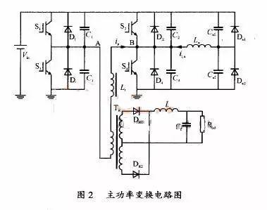
The above figure shows topological diagram of a phase-shifted full bridge. Each component has following meaning:
Vin: DC power input
T1-T4: 4 main switch lamps, usually MOSFET or IGBT
T1, T2 are called forearm switching super tubes, T3, T4 are called lagging arm switching tubes
C1-C4: Parasitic capacitance of 4 switching lamps or additional resonant capacitance
D1-D4: Parasitic diodes of 4 switching lamps or additional freewheel diodes
VD1, VD2: power secondary high-frequency rectifier diode
TR: full-bridge phase-shifting power transformer
Lp: transformer primary inductance
Ls1, Ls2: Secondary transformer inductance
Lr: primary transformer leakage inductance or sum of primary leakage inductance and external inductance
Lf: phase shifted full bridge secondary output inductance
Cf: Secondary output capacitance of phase shift bridge power supply
RL: phase-shifted full-bridge power supply secondary load
Since this is a theoretical analysis, it is necessary to idealize characteristics of some devices as follows:
1. Assuming all switches are ideal components, there are no turn-on and turn-off delays, and on-state resistance is infinitely small, internal diode or outer diode of switch is also an ideal component, and there is no turn-on and turn-off delay. The forward voltage drop is 0.
2. All inductors and capacitors are ideal components, there are no parasitic parameters, transformer is also an ideal transformer, there is no influence of leakage inductance and distribution parameters, excitation inductance is infinite, excitation current can be neglected. , and resonant inductance is external.
3. The leading arm of bridge and lagging resonant capacitance are equal, that is, C1=C2=Clead, C3=C4=Clag.
The free-wheeling secondary inductance converted to primary inductance LS` through turn factor is much larger than resonant inductance Lr, that is, LS=Lr*n2》Lr.
One PS FB cycle can be divided into 12 working modes, among which positive and negative half cycles are corresponding ratios, but what changes is direction of current on bridge arm. Let's analyze these 12 working modes. First, in this situation, mystery of out-of-phase full bridge is revealed.
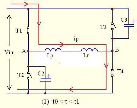
Half-cycle positive power output process
As shown in figure above, at this time, T1 and T4 are turned on at same time, T2 and T3 are turned off at same time, and direction of primary side current is T1-Lp-Lk. -T4 as shown in picture.
The input voltage at this time almost completely falls on two points A and B in figure, that is, UAB=Vin. At this time, inductance of two points AB should be in addition to Lp and Lk is marked in figure. turn ratio, so LS` will be much larger than Lk, causing Ip to rise slowly, and rising current △Ip is △Ip=(Vin-n*Uo)*(t1-t0)/(Lk+ LS`)
Vin-n*UO is voltage across resonant inductor, which is input voltage minus secondary reflected voltage.
At same time, according to ratio between same terminals of transformer, secondary diode VD1 turns on, and VD2 turns off. The primary side of transformer provides power to load, but at same time stores energy for output choke Lf and output capacitor Cf. (not shown)
Currently UC2=UC3=UA=UAB=Vin UB=0V

Super Resonant Forearm Process
As shown in figure above, at this time, upper tube T1 of leading arm of bridge is off at time t1, but because current at both ends of inductor cannot change, current to primary side of transformer must still maintain original direction, so current is transferred to C1 and C2, C1 is charging and voltage will soon rise to input voltage Vin, while C2 starts to discharge and voltage will soon drop to 0, that is, potential of point A is clamped to 0V.
Since inductance LS` converted from secondary winding is much larger than inductance Lk of resonant inductor, it can basically be considered that primary side of this is similar to a DC source, and ip at this time is basically unchanged or drops very slightly .
The voltage across C1 is given by expression
Vc1=Ip*(t2-t1)/(C1+C3)= Ip*(t2-t1)/2 Clead
The voltage across C2 is given by expression
Vc1= Vin-【Ip*(t2-t1)/2 Clead】
Where Ip is current flowing through primary inductor in mode 2, voltage across C1 rises rapidly to Vin at T2, voltage across C2 quickly becomes 0V and D2 begins to conduct.
Until t2, C1 is fully charged and C2 is fully discharged, i.e. VC1= VC3= Vin VC2=VA=VB= 0V
Mode 2 time is △t= t2-t1=2 Clead * Vin/ Ip
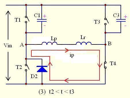
Primary freewheel positive half-cycle current
As shown in figure above, at this time, diode D2 has fully turned on free running, and voltage at both ends of lower tube of super forearm T2 is fixed at 0 V. At this time, T2 is turned on, and opening of ZVS of lower tube of T2 super forearm is realized, but at this time, primary current is still flowing from D2 instead of T2.
At this time, current flowing through primary side is still relatively large, and secondary side inductance current Lf is converted to primary side current, that is, ip(t)= iLf(t) / p
Currently, rate of current drop is related to inductance.
The period td from turning off super-forearm T1 to opening T2 is called dead zone time of super-forearm.
td ≥△t= t2-t1=2 Clead * Vin/ Ip
Currently UC1=UC3=Vin, UA=UB=UAB=0V
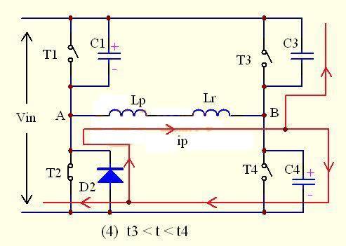
Positive half-cycle resonant process with delayed shoulder
As shown in figure: turn off lower tube T4 of lagging arm at point T3, before turning off T4, voltage at both ends of C4 is 0, so T4 turns off with zero voltage.
Due to T4 disconnection, primary current ip suddenly loses its path, but from principle of inductance, we know that primary current cannot change abruptly, and it must maintain its original direction and decrease at a certain rate. Therefore, primary current ip will charge C4 so that voltage at both ends of C4 will slowly rise and at same time charge at both ends of C3 will be drained.
That is, ip(t)=I2sinω(t-t3)
vc4(t)=ZpI2sinω(t-t3)
vc3(t)=Vin-ZpI2sinω(t-t3)
Among them I2: value of current after fall of primary current at time t3
Zp: resonant impedance of lagging arm, Zp= )0.5
ω: lagging arm resonant angular frequency, ω=1/(2Lr*Clag)0.5
Some people may wonder why current has a sinusoidal function, yes, because at this time resonant inductance Lr of primary side resonates with two capacitors C3 and C4 of lagging arm, and dependence is a sinusoidal dependence. .
Why did I mention above that only resonant inductance Lr on primary side participates in resonance, while secondary energy storage inductance participates in resonance? Let's analyze it below:
Due to disconnection of lower tube T4 of lagging arm, C4 slowly builds up voltage and finally equals voltage of power supply, i.e. UC4 = Vin. It can be seen from figure that UC4 is actually voltage at point B and at both ends of C4 The voltage rise is process of slowly increasing voltage at point B from 0V, and at this time voltage at point A is fixed at 0V, so this will lead to fact that UAB<0 V, i.e., we can say that at this time voltage of primary winding began to change.
Due to reverse voltage of primary side, according to ratio between same terminals, LS1 and LS2 have both positive and negative ratio. The current from VD1 cannot be immediately reduced to 0, but it can only decrease slowly, and current through VD2 can only be slowly increased, so a situation arises when VD1 and VD2 are turned on at same time, that is, secondary windings LS1 and LS2 are simultaneously turned on. is a short circuit.
A short circuit of secondary winding cuts off reflection path Lf to primary side, that is, primary side inductance to participate in resonance will quickly decrease from original (Lf * n2 + Lr) only to Lr. Since Lr is much smaller than (Lf*n2+ Lr), primary current will decrease rapidly.
Currently UAB=ULr=-Vin of primary side, UA=0V, UB= Vin

Resonance has ended and primary inductance feeds power into network
As shown in figure, when C4 is charged to Vin, resonance ends, and no current flows through C3 and C4, but D3 turns on naturally, and primary current supplies energy to grid through D2-Lr-D3. .In fact, energy comes from energy stored in Lr, at this time, primary current decreases rapidly,
ip(t)= Ip4-(t-t4)
where Ip4 is main value of current at time t4
Reduces to 0 at time t5.
At this time, voltage drop across T3 is 0V. As long as T3 is turned on at this time, T3 will achieve zero-voltage turn-on effect.
Here you need to introduce several concepts:
Dead time: Super forearm or lagging arm upper and lower tubes, time interval between on or off, full phase shift bridge power supply has 4 dead times per cycle.
Resonance period: after turning off two lagging arm lamps and before switching on two super-arm lamps, sum of inductance reflected by secondary inductance through turn factor, resonant inductance and two resonance times of respective resonant capacitors; There are two resonance times between resonant inductor and their respective resonant capacitors before super-arm is opened and two tubes of lagging arm commute.
Phase angle: refers to time interval from opening of upper tube of forearm to opening of lower tube of lagging arm, or interval of time from opening of lower tube of anterior forearm to opening of upper tube of lagging arm, and then converted to angular frequency ω
ω=2∏f=2∏/T.
For switching mode 5, resonance period must be less than dead time, otherwise ZVS lagging arm effect cannot be achieved. But at this time, resonant inductance does not have a secondary inductance reflected back through turning factor, so only resonant inductance is involved in resonance. Be careful when designing, resonant inductance must be large enough, otherwise if resonance energy is not enough, primary current will be reduced.
At time t5 UAB=ULr=-Vin, UA=0V, UB= UC1= Vin
Primary current increases from 0 in reverse order
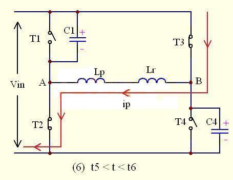
As shown in figure, T3 was on until time t5, and current ip of primary side at time t5 dropped to 0. Since there is no current, D2 and D3 are naturally turned off.
For a period of t5-t6, diodes D1 and D2 on secondary side are still conducting, shorting secondary winding and blocking output inductance from reflecting back to primary. , load current still comes from secondary level inductance and output capacitance; at same time, since T2 and T3 of primary side are turned on, primary current ip flows through T3--Lr--T2, and since Lr is very small, primary current ip will rise sharply.
That is, ip(t)= - (t-t5)
At time t6 ip reaches a maximum which is equal to primary current converted from current of inductor on secondary side
That is, ip(t6)= - ILf(t6)/n
In this switching mode, primary current does not transfer energy, but a violent switching process occurs on secondary side. The current through secondary diode VD1 decreases rapidly, and current VD2 increases rapidly. At t6, current through VD1 decreases to 0, and current through VD2 is equal to current of inductor ILf.
Until t6 UAB= ULr=-Vin on primary side, UA=0V, UB= Vin
After time t6, positive half-cycle of phase-shifted full bridge ends and negative half-cycle begins. Its principle of operation is similar to the positive half-cycle. further analysis below:
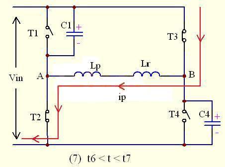
Negative output power half cycle
As shown in figure above, at this time, T2 and T3 are turned on at same time, T1 and T4 are turned off at same time, primary current flow direction is ip: T3-Lk-Lp-T2, as shown in figure.
The input voltage at this time almost completely drops at two points B and A in figure, i.e. UAB=-Vin. LS`=n2* Lf because it is converted back according to square of gear ratio, so LS` will be much larger than Lk, causing Ip to grow slowly, and growth of current △Ip is -△Ip=-【( Vin-n*Uo)*(t7-t6)/(Lk+LS`)】
During this process, according to ratio between same terminals of transformer, secondary diode VD2 turns on and VD1 turns off. The primary side of transformer supplies energy to load, and at same time stores energy for output choke Lf and output capacitor Cf. (not shown)
Currently UC1 =UC4=UB =Vin UAB=-Vin UA=0V
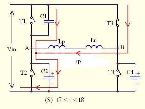
Negative half-cycle forearm superresonance process
As shown in figure above, at this time, lower tube T2 of bridge driving arm is off at time t7, but because current at both ends of inductor cannot change, current on primary side of transformer still needs to be maintained original direction, so current is transferred to C1 and C2, C2 is charging and voltage will soon rise to input voltage Vin, while charge of C1 will be drawn out quickly will disappear, and voltage at both ends of C1 will soon drop to 0V, that is potential of point A will be clamped on Vin.
Since inductance LS` converted from secondary winding is much larger than inductance Lk of resonant inductor, it can basically be considered that primary side of this is similar to a DC source, and ip at this time is basically unchanged or drops very slightly .
The voltage across C2 is given by expression
Vc2=︱-Ip︱*(t8-t7)/(C1+C2)= Ip*(t8-t7)/2 Clead
The voltage across C1 is given by expression
Vc1= Vin- 【︱-Ip︱*(t8-t7)/2 Clead】
Where Ip is current flowing through primary inductor in mode 8, until time t8 voltage across C2 rapidly rises to Vin, voltage across C1 quickly becomes 0V and D1 begins to conduct.
Until t8, C2 is fully charged and C1 is fully discharged, i.e. VC2= VC4=VA=VB = Vin VC1=VAB= 0V
Time for modal 8
△t= t8-t7=2 Clead * Win/Yip
Note: The time △t must be less than dead time, otherwise it will affect ZVS effect.
The 4th and 8th operating modes are resonant modes of lagging arm and super forearm, respectively, and detailed analysis process will be described later
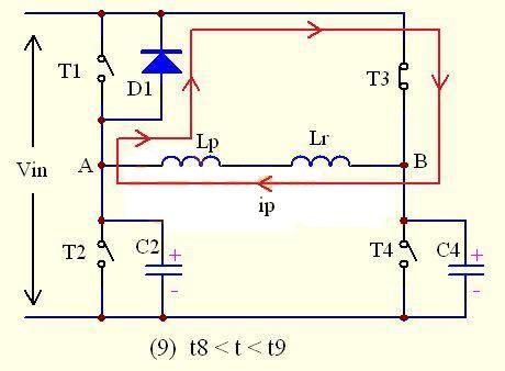
Primary Side Current Negative Half Cycle Clamp Freeplay Process
As shown in above figure, at time t8, diode D1 fully turned on at idle, clamping voltage at both ends of upper super-arm transistor T1 to 0 V and turning on T1 at that time, realizing opening of ZVS. upper transistor of super-forearm T1; but at this time primary current is still flowing from D1 instead of T1.
At this time, current flowing through primary side is still relatively large, and secondary side inductance current Lf is converted to primary side current, that is, ip(t)= iLf(t) / p
At this time, rate of current drop is related to inductance of secondary inductor.
The period td from switching off super forearm T2 to opening T1 is called dead zone time of the super forearm.
td ≥△t= t9-t8=2 Clead * Vin/ Ip
Currently UC2=UC4=UA=UB=Vin, UAB=0V
Negative half-wave resonant process with lagging arm
As shown in figure: turn off upper tube T3 of lagging arm at T9, and before T3 is turned off, voltage at C3 is 0, so T3 refers to zero voltage cut-off.
Due to T3 disconnection, primary current ip suddenly loses its path, but from principle of inductance, we know that primary current cannot change abruptly and must maintain its original direction and decrease at a certain rate. Therefore, primary current ip will charge C3, causing voltage across C3 to rise slowly, and at same time C4 begins to discharge. That is, ip(t)=-I2sinω(t-t9)
vc3(t)=Zp*︱-I2︱sinω(t-t9)
vc4(t)=Vin-Zp*︱-I2︱sinω(t-t9)
Among them -I2: instant t9, current value after current drop on primary side
Zp: resonant impedance of lagging arm, Zp= )0.5
ω: lagging arm resonant angular frequency, ω=1/(2Lr*Clag)0.5
Similarly, resonant inductance Lr on primary side resonates with two capacitors C3 and C4 of lagging arm, and relationship between voltage and current is sinusoidal.
Similar to four switching mode analysis, due to reverse voltage on primary side, according to relationship between same terminals, LS1 and LS2 have ratio of upper positive and lower negative at same time, at this time VD1 starts conduct and flow current; and Due to relationship between LS2 and Lf, current flowing through LS2 and VD2 cannot be reduced to 0 immediately, but can only decrease slowly; and current through VD1 can only increase slowly, so VD1 and VD2 turn on simultaneously, with secondary windings LS1 and LS2 shorted simultaneously.
A short circuit of secondary winding cuts off reflection path Lf to primary side, that is, primary side inductance to participate in resonance will quickly decrease from original (Lf * n2 + Lr) only to Lr. Since Lr is much smaller than (Lf*n2+ Lr), primary current will decrease rapidly.
At time t10 UAB=ULr=Vin on primary side, UB=UC4=0V, UA=UC2=UC3=Vin
The resonance ends and primary inductance supplies energy to network
As shown in figure, when C3 is charged to Vin, resonance ends and no current flows through C3 and C4, but D4 turns on naturally, and primary current supplies energy to grid through D4-Lr-D1. , Its energy comes from energy stored in Lr, at this time, primary current decreases rapidly,
ip(t)= -【Ip10-(t-t10)】
where Ip10 is value of primary current at time t10
Reduces to 0 at time t11.
At this time, voltage across T4 drops to 0V. As long as T4 is turned on at this time, T4 will achieve effect of turning on at zero voltage.
For switching mode 11, resonance period must be less than dead time, otherwise lagging arm ZVS effect cannot be achieved. But at this time, resonant inductance does not have a secondary inductance reflected back through turning factor, so only resonant inductance is involved in resonance. Be careful when designing, resonant inductance must be large enough, otherwise if resonance energy is not enough, primary current will be reduced.
At time t11 UAB=ULr= UC3=UA=Vin, UB=0V

Primary current increases from 0 to positive
As shown in figure, T4 was on until time t11 and primary current ip rose to 0 at time t11. Since there is no current, D1 and D4 are naturally off.
During period t11-t12, diodes D1 and D2 on secondary side are still conducting, shorting secondary and blocking output inductance from reflecting back to primary. , load current still comes from secondary winding. At same time, since T1 and T4 of primary side are turned on, primary current ip flows through T1--Lr-T4, and since Lr is very small, primary current ip will increase sharply in positive direction.
That is, ip(t)= - (t-t11)
At time t12 ip reaches a maximum which is equal to primary current converted from inductor current on secondary side
That is, ip(t12)= - ILf(t12)/n
In this switching mode, primary current does not transfer energy, but a violent switching process occurs on secondary side. The current through secondary diode VD2 decreases rapidly, and current VD1 increases rapidly. At t12, at this moment, current through VD2 decreases to 0, and current through VD1 becomes equal to current of inductor ILf.
At time t12 UAB= ULr=UA=UC3=Vin, UB= 0 V on primary side
A full duty cycle analysis of a complete bridge with phase shift has now been completed.
Some of them may be slightly incorrect (corrections are welcome), but this does not affect general principle of operation. I first presented 12 modes of operation in form of drawings. For ease of analysis, I omitted Analysis of secondary winding loop
12 working processes include: 2 positive and negative output power half cycles, 2 positive and negative half cycles, clamp free running processes, 4 resonant processes (including 2 bridge shoulder resonant processes and 2 flux switching processes), two primary side accumulation energy of inductance is returned to network process, and finally there are two current drops on primary side of transformer or a zero crossing to complete rapid change process. These 12 processes make up full duty cycle of full phase shift bridge. If any process deviates or is abnormal, it will affect ZVS effect of full phase shift bridge, and even cause entire power supply to fail. work fine.
Problems with full bridge with phase shift
Problem 1: It is difficult for lagging hand to reach ZVS
Reason:
When lagging arm resonates, short circuit of secondary winding is clamped, so inductance of secondary side cannot be reflected to primary side to participate in resonance, and resonance energy can only be provided by resonant inductor. If there is not enough energy, then there will be no lagging voltage resonant condensera sator connected in parallel with hand tube resonates to 0V.
nSolution:
① Increase excitation current. But this will increase losses of devices and transformers.
②, increase resonant inductance. But this will cause a more serious duty cycle loss of secondary side.
③. Add an auxiliary resonant network. But this will increase cost and volume.
nQuestion 2:
Loss of Secondary Duty Cycle
Reason:
There is a serious switching process in current of primary side of a full bridge with a phase shift. At this time, current of primary side is not enough to provide load current of secondary side, so inductance of secondary side will conduct another diode to continue current, that is, secondary side of edge is approximately in a short circuit state;
Dloss is proportional to resonant inductance and load RL and inversely proportional to input voltage.
nSolution:
①. Decrease rotation ratio of primary and secondary sides. However, this will increase withstand voltage of secondary rectifier lamp.
② Change resonant inductance to saturable inductance. Because in process of primary switching, once it enters saturation state of inductor, current flowing through inductor will immediately become saturation current instead of decreasing linearly, which means that switching time is reduced, which is equivalent to reducing Duty cycle is wasting time. Of course, my explanation seems a bit difficult to understand. It must be understood in conjunction with working process of a phase-shifting full bridge. You can still experience it slowly
Insert PSFB magnetic device calculation method.
n Construction of output energy storage inductor:
A full-bridge phase-shift energy storage choke can actually be thought of as a simple BUCK choke. Because its positive and negative half-cycles operate once each, its operating frequency is twice switching frequency. The calculation formula is:
Lf = Vo *(1-Dmin)/(4*fs* △I)
Lf in above formula represents minimum inductance. The actual value must be greater than this value to ensure current continuity. If output voltage needs to be constantly adjusted within a certain range, Vo must be Vo (min.), i.e.
Lf = Vo(min) *(1-Dmin)/(4*fs* △I)
The Dmin formula above is provided for ease of understanding. In fact, duty cycle of a full phase-shifted bridge is unchanged and there is no minimum duty cycle:
Dmin= Vo(min)/(Vin(max)/n-VLf-VD)
n Construction of main transformer:
First, calculate minimum secondary output voltage of a phase-shifted full bridge:
Vsec(min)=( Vo(max)+VLf+VD)/ Dsec(max)
The ratio of turns of primary and secondary transformers:
n=Vin(min) /Vsec(min)
Select a converter and use Ap method:
Ap =Ae*Aw= Po*104 /(4*ƞ*fs*△B*J*Ku*)
Next, calculate number of turns on primary winding of transformer:
Np= Vin(min)*D(max)/(4*fs*Ae*Bmax)
Then number of turns in secondary winding:
Ns= Np/n
n resonant inductor design:
The purpose of adding a resonant inductor is to implement a ZVS lagging arm switching tube. As in previous analysis, when lagging arm resonates, secondary inductance cannot be reflected back to primary through transformer. in order to ensure ZVS of lagging arm switching tube, resonant inductance Energy must satisfy following formula:
LrIp2/2=(Vin2*C top tube)/2+(Vin2*C bottom tube)/2= Vin2*Clag
i.e. Lr= 2* Vin2*Clag /Ip2
where Lr: value of resonant inductance
Vin: input voltage
Clag: lagging bridge arm capacitance (external capacitance and MOSFET junction capacitance)
Ip: primary side current when lagging bridge arm is switched off
The following factors are also taken into account in calculation:
①.Vin must take highest input voltage value to ensure that lagging bridge arm can reach ZVS at any input voltage.
② Considering that at time of low load Ip1 (10%-20% load), lagging axle arm must still operate in ZVS state.
③.When output current iLf is at a certain value (such as 2A), output current of energy storage inductor is still continuous or at a critical point.
That is, ripple current of energy storage output inductor is twice this value
That is △ iLf = 2 *2A=4A
Then Ip=(Ip1+ △iLf /2)/
Related
- (Detailed long article) Detailed interpretation of twelve modes of operation of a phase-shifted full bridge.
- Detailed and detailed explanation of ripple current value of inductance of power supply BUCK r
- Detailed analysis of the "various protection schemes" of a switching power supply
- A detailed explanation of role of pull-up resistors on triodes and MOS lamps.
- The composition of switching power supply circuit and a detailed explanation of general circuits
- [Comic] Detailed explanation of knowledge of power sources
- A detailed explanation of three commonly used LED drive power schemes.
- Detailed explanation of working principle of TTL gate circuit
- A detailed explanation on how to select inductor value of the DC boost converter.
- Detailed explanation of commonly used LED drive power
Hot Posts
 How to distinguish induction from leakage, we will teach you three tricks! Ordinary people can also learn super practical
- What is drowning in gold? Why Shen Jin?
- This is a metaphor for EMI/EMS/EMC that can be understood at a glance.
- How many types of pads have you seen in PCB design?
- Summary of Common PCB Repair Techniques
- What is three anti-paint? How to use it correctly?
- Knowing these rules, you will not get confused looking at circuit diagram.
- How to make anti-interference PCB design?
- Can diodes do this?