Location:Home Page > Archive Archive
A detailed explanation of role of pull-up resistors on triodes and MOS lamps.
2023-03-18【Archive】
About triode
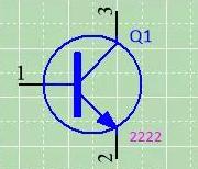
A brief explanation on triode, if triode operates in saturation region (fully turned on), Rce≈0, Vce≈0.3V, and this is 0.3V, then we think it is directly grounded. Then it is necessary to make Ib greater than or equal to 1mA if Ib=1mA, Ic=100mA, its gain is β=100, and triode is fully on. As shown in the figure below, this is an NPN transistor.
The triode is a current-type drive component, so normally a current-limiting resistor is in series with base, typically less than or equal to 10K, but why is there a pull-up resistor in base? For example. The following figure shows circuit diagram of temperature switch control motor.
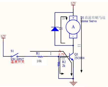
As shown in figure, temperature switch controls start and stop of motor. The temperature switch is similar to push button switch. The switch is connected in series to pole B and tube N can be used as a switch tube. The motor in picture is a brushed DC motor. As long as positive pole is connected to 12V and negative pole is grounded, motor will start to rotate.
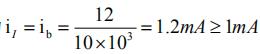
When temperature switch is turned on, current flowing through circuit I is equal to
The CE triode is fully on, Vce » 0.3V, at this time voltage drop across motor is close to 12V and it can rotate because impedance of triode be is much smaller than 2K resistor R2, so most of current flows through triode, when thermal switch is turned off, there will be no current in ib, and there will be no current in ic.
Because at moment thermal switch is turned off, current on triode ib and ic cannot immediately drop to zero, but slowly drops to zero. This is inevitable existence of production process. During this time, triode operates in amplification zone and is most susceptible to interference. Therefore, it is necessary to connect a pull-up resistor R2, which, firstly, provides a discharge circuit for triode, and secondly, provides an energy dissipation path for point A.
How to understand discharge pattern?
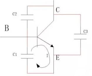
As shown in figure below, triode parasitic capacitance, actual model of triode manufacturing process, has capacitances C1, C2, and C3 between triodes BE, BC, and CE, respectively. The existence of these three capacitors is, on one hand, unnecessary for us, and on other hand, it is inevitably overcome in process, and is an inevitable phenomenon in production process. We usually refer to this capacitance as parasitic capacitance or parasitic capacitance.
Due to presence of capacitance, triode will necessarily have a delay. In absence of current in ib, capacitor C1 begins to discharge, forming a loop I. At this time, voltage at point B drops from 0.7V to 0V. It operates in amplification zone and is most prone to interference. Add a resistor R2 at both ends of C1. Resistor R2 therefore provides a way for capacitor to shed charge, greatly reducing triode's operating time in the amplification zone.
How do you understand providing a decentralized path for energy?
Why is resistor R2 said to provide a power dissipation path for point A. As shown in figure 2, when temperature switch is turned off, point A is suspended at that time, voltage at point A is unknown, and it is in a state of high impedance (infinite impedance), which is prone to false conduction. and is also subject to environmental influences such as static electricity, lightning strikes, etc. may permanently damage device.
When lightning strikes, high-voltage static electricity, etc. in working environment, lower resistor at point A and connect it to ground, and most of current will flow to ground along resistor, providing an energy dissipation path. If this resistor is not connected, when lightning strikes, since impedance on left side of point A is infinite, and right side of point A is connected to triode, impedance is very low compared to left side, so all current will flow in low impedance direction and flow into triode , causing a current. If it is too large, device will be irreversibly damaged.
About MOS tube
Due to space constraints, a basic knowledge of MOS lamps can be found here: MOS Lamp Basics.
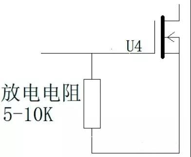
The pull-up resistor has two functions:
In order to prevent release of charge by static electricity, it is easy to cause electrostatic breakdown
When MOS lamp is running in switching state, there is a continuous charge and discharge of Cgs. When power is turned off, part of charge can be stored in Cgs, but there is no reset circuit, and electric field of MOS lamp gate is still there and can last a long time conditions for establishing a conductive channel did not disappear. The next time current-carrying channel is started, MOS lamp immediately generates an uncontrolled huge drain current Id, causing MOS lamp to burn out.
Related
- A detailed explanation of role of pull-up resistors on triodes and MOS lamps.
- A detailed explanation of three commonly used LED drive power schemes.
- [Comic] Detailed explanation of knowledge of power sources
- What is a delay scheme? Explanation of 6 Kinds of Delay Circuit Principles
- Detailed analysis of the "various protection schemes" of a switching power supply
- The role of polar and non-polar capacitors in parallel connection
- Summary of questions and answers on basics of analog circuits
- MOS tube drive circuit, how to make MOS tube turn on and off quickly?
- "Easy to understand" Miller effect when switching MOS lamps
- Diodes, triodes, MOS tubes, commonly used physical package map (including exact dimensions)
Hot Posts
 How to distinguish induction from leakage, we will teach you three tricks! Ordinary people can also learn super practical
- What is drowning in gold? Why Shen Jin?
- This is a metaphor for EMI/EMS/EMC that can be understood at a glance.
- How many types of pads have you seen in PCB design?
- Summary of Common PCB Repair Techniques
- What is three anti-paint? How to use it correctly?
- Knowing these rules, you will not get confused looking at circuit diagram.
- How to make anti-interference PCB design?
- Can diodes do this?