Location:Home Page > Archive Archive
The practice of designing switching power supplies of low power
2023-11-28【Archive】
This chapter takes design of a small-sized power supply as an example to illustrate power supply design method. The shape of control circuit corresponds to type of its excitation, and UC3842 is used as PWM control circuit. The choice of power switching frequency determines characteristics of converter. The higher switching frequency, smaller transformer and inductor, and better dynamic response of circuit. However, as frequency increases, losses such as switching losses, gate drive losses, and output rectifier losses become more pronounced, and requirements for selection of magnetic materials and sizing become more stringent. In addition, degree of influence of line parasitic parameters on line at high frequencies is unpredictable, and stability, performance and system debugging of entire circuit will be difficult. In this power supply, an operating frequency of 85 kHz is selected.
1. Power supply design indicators
The input and output parameters of small power supply are as follows:
Input voltage: 110/220 VAC;
Input voltage range: 90~240V;
Input frequency: 50/60 Hz;
Output voltage: 12V;
Output current: 2.5A.
Second, choice of schema structure
A single-ended flyback or single-ended forward circuit can be used for a low-power switching power supply, making power supply simple in design, reliable in operation, and inexpensive. Compared with single-ended flyback circuit, single-ended forward circuit has small switching current, small output ripple, and can more easily adapt to high frequency. The basic circuit of a single-ended direct switching power supply consisting of a UC3842 PWM current control IC is shown in Figure 6-1.
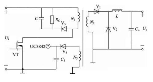
Figure 6-1. The main circuit of a single-ended switching power supply of forward stroke
The direct switching single-ended switching power supply is equipped with a magnetic flux shedding circuit to release energy of excitation circuit. In Figure 6-1, when VT switch lamp is turned on, V1 is on, secondary winding of N2 is feeding load, V4 is off, and feedback coil current of N3 is zero, when VT is turned on, V1 is off, V4 is on, and N3 passes through capacitor C1 after filtering supplies power to pin ⑦ of UC3842, and at same time, induced electromotive force generated in primary winding of N1 causes V3 to conduct and add it. to RC absorption chain. Since energy of magnetic field in transformer can be discharged through N3, unlike general RC D magnetic flux dump circuit, it is consumed at resistor, so this can reduce heat and improve efficiency.
Third, component design
1) Construction of transformer and output inductorAccording to application method of UC3842, select timing resistor RT=1.8kΩ and timing capacitor CT=10uF. Determine switching frequency f = 85 kHz, period T = 11.8 µs. When designing an asymmetrical switching power supply, maximum duty cycle D usually does not exceed 0.5. Here D=0.5 is selected, then: 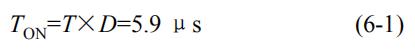
Select PQ26/25 core according to power supply specification, output power and switching frequency. The cross-sectional area of the core is S=1.13cm2, effective length of core is l=6.4cm, and saturation flux density is BS=0 .4 T Assuming maximum working strength of magnetic induction of transformer Bmax = BS / 3≈0.133 T, then inductance coefficient A is: 
The number of turns N1 of primary winding of transformer is: 
In formula, Ui is minimum DC input voltage. The minimum value of input AC voltage is about 90 V, Ui = 90 × ≈ 127 V, N1 = 49.9 turns, and 50 turns are taken. Primary coil inductance L = AN12 = 11.1 mH.
Number of turns of secondary winding: 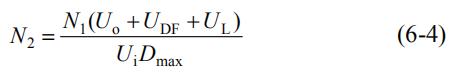
In formula, UDF is voltage drop across rectifier diode V1, UL is voltage drop across output inductor L. We take UDF+UL=0.7 V, substitute it into formula (6-4), we get N2=10 turns. Secondary coil inductance: 
When switch tube is disconnected, an induced electromotive force will be generated at both ends of N1. To ensure normal operation of switch tube, induced electromotive force is limited to e=300 V. The electrical feedback coil provides an operating voltage of U=12 V for UC3842, calculated voltage UC=16V across capacitor C1 to provide sufficient supply voltage for UC3842. N3 = 2.67 turns can be obtained from N3 = (UC/e) N1, take 3 turns. The secondary current of transformer is a square wave, its effective value: 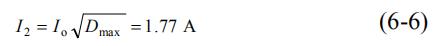
The current density of wire is 4A/mm2, and cross-sectional area of the winding wire required is 1.77/4≈0.44mm2. You can also select primary wire, RMS primary current: 
The cross-sectional area of the winding wire required is 0.354/4=0.0885 mm2, and a wire with a cross-sectional area of 0.096 21 mm2 (∅0.41 mm) is selected. Take current change in output inductance ΔIL=0.2Io=0.5A, then output inductance is: 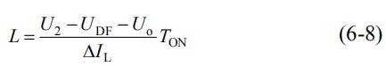
In formula, U2 is minimum voltage of secondary winding. Calculated: 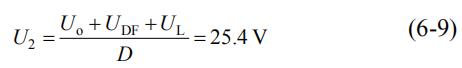 UDF = 0.5 V, Uo = 3 V, and substituting in formula (6-8), we get L = 140 μH. For current IL=Io at output inductance, required cross-sectional area of the winding wire should be 2.5/4=0.625 mm2, so a wire with a cross section of 0.6362 mm2 (∅0.96 mm) was selected. 2) Switching tube, rectifier diode and flyback diode selection Since induced electromotive force at both ends of primary winding N1 is limited to eL≈300V when switching tube is turned off, after full-wave rectification of input AC voltage and capacitor is filtered, maximum value of DC input voltage.
So maximum reverse voltage that a rectifier diode can handle is: 
The maximum reverse voltage that a reverse diode can withstand is: 
The maximum current flowing through rectifier diode and flyback diode is: 
Get ID = 2.75A. Based on above calculation, Schottky half-bridge MBR25120CT is selected, average rectified current 25A, reverse peak voltage 120V. 3 A.
3) Feedback circuit designThe current feedback circuit uses a current transformer and detects switch tube current as sampling current. The principle is shown in Figure 6-2. The current transformer output is divided into two instantaneous current feedback and average current feedback circuits, and voltage across resistor R2 reflects instantaneous current value. Changing current on switch tube will change UR2, and UR2 is connected to protection input terminal ③ of UC3842 pin. When UR2 = 1V, output pulse of UC3842 chip will be turned off. By adjusting voltage division ratio of R1 and R2, current limit value of switching tube can be changed to realize a cycle-by-cycle comparison of instantaneous current value that belongs to current limiting protection. The output pulse is disabled to implement average current protection, which is related to cutoff protection.
The two overcurrent protections complement each other, making power supply safer and more reliable. The current transformer sampling is used to isolate control circuit from main circuit, and at same time, compared with resistance sampling, power consumption is reduced, thus improving efficiency of entire power supply.
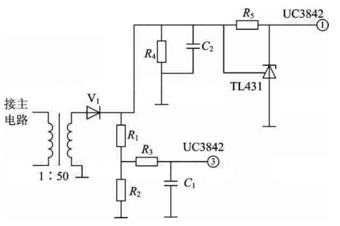
Figure 6-2 Current Feedback Circuit
The voltage feedback circuit is shown in fig. 6-3. The output voltage is fed back to ① pin of UC3842 through built-in TL431 voltage regulator and optocoupler, and output voltage can be set and adjusted by adjusting voltage division ratio of R1 and R2 to achieve higher voltage regulation accuracy. When output voltage Uo increases, current from cathode to anode of built-in voltage regulator TL431 increases, which increases triode current at output of optocoupler, that is, shunt of output ① of UC3842 to ground becomes larger, and output pulse width of UC3842 decreases accordingly, output voltage Uo decreases. Similarly, if output voltage Uo decreases, it can be increased by closed-loop control.
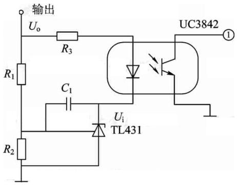
Figure 6-3 Voltage Feedback Circuit
4) Construction of protection circuit
In fig. Figure 6-4 shows transformer overtemperature protection circuit, and NTC is an NTC thermistor for measuring transformer temperature. The hysteresis comparator consists of NTC, R2 and op amp A1. Under normal operation, temperature of transformer is normal, NTC resistance is relatively large, voltage U+
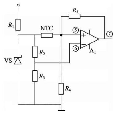
Figure 6-4 Transformer overtemperature protection diagram
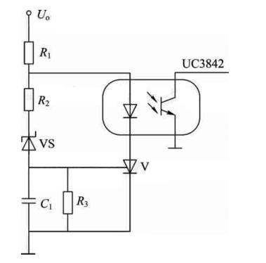
Figure 6-5 Output Surge Protection Circuit
In fig. Figure 6-6 shows idle protection circuit. In order to prevent too high voltage on transformer winding, as well as to reduce load effect of power supply from no-load to full load, output end of switching regulated power supply should not be open. On fig. 6-6, resistors R2 and R3 supply a fixed voltage U+ to non-inverting input of op-amp. R8 is a shunt to sample load current. When external circuit is not connected to load RL, there is no current on R8, and voltage at inverting input of operational amplifier is U=0 V, so U+> U-, and output voltage of op-amp is higher. The triode VT saturates and turns on, and dummy load R7 inside power supply is automatically connected. When power supply is connected to load RL, voltage drop across R8 is U-> U +, output voltage of operational amplifier is zero, VT is disabled, R7 is disabled.
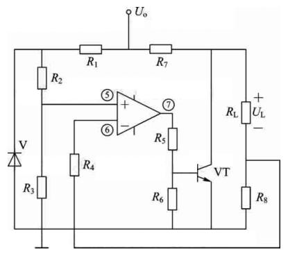
Figure 6-6 Idle protection circuit
5) Design of input filter circuit
The input filter circuit has a two-way isolation function, which can suppress AC mains noise input signal, as well as prevent harmonics and EMI signals generated during operation of switching power supply from affecting AC mains. . The filter circuit shown in Figure 6-7 is a composite EMI filter L1, L2 and C1 constitute first filtering stage, and common mode inductor L3 and capacitors C2 and C3 constitute second filtering stage. C1 is used for differential noise filtering, and a film capacitor with best high-frequency performance is selected. Resistor R provides a capacitor discharge circuit to avoid filter performance being affected by charge buildup on capacitor. C2 and C3 are connected to output end, which can effectively suppress common mode interference. To reduce leakage current, ceramic capacitors should be used in C2 and C3.
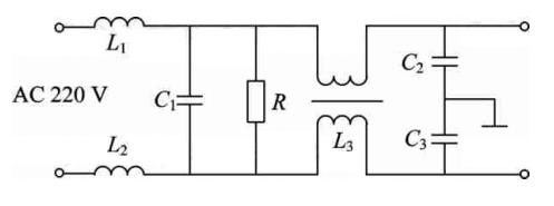
Figure 6-7 Input filter circuit
Fourth, check
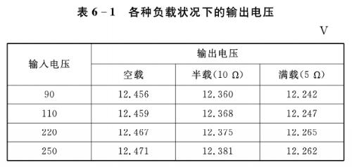
When input voltage is 220V, input power is a pulse train with a cycle of 10ms, that is, every half cycle of mains frequency, power input terminal charges input smoothing filter capacitor once through rectifier bridge. Under various load conditions, when input voltage changes from 90V to 250V, test results of corresponding output voltage are shown in Table 6-1.
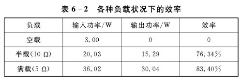
The measured efficiency under various load conditions is shown in Table 6-2. Due to practical application, power supply meets design requirements.
Related
- The practice of designing switching power supplies of low power
- Detailed analysis of the "various protection schemes" of a switching power supply
- The composition of switching power supply circuit and a detailed explanation of general circuits
- Research "Exchange of haberdashery" technology of parallel connection of high-power DC and DC power supplies of IGBT devices.
- The best switching circuit design process for power supplies is a must for engineers!
- The distribution parameters for magnetic components should be used by specialists in switching power supplies.
- Four ways to reduce the output "ripple and noise" of a switching power supply
- Analysis of damping RC circuit of a switching power supply "haberdashery"
- Detailed analysis of various losses in switching power circuits
- A collection of basic schematic diagrams of power supplies, an indispensable book for engineers.
Hot Posts
 How to distinguish induction from leakage, we will teach you three tricks! Ordinary people can also learn super practical
- What is drowning in gold? Why Shen Jin?
- This is a metaphor for EMI/EMS/EMC that can be understood at a glance.
- How many types of pads have you seen in PCB design?
- Summary of Common PCB Repair Techniques
- What is three anti-paint? How to use it correctly?
- Knowing these rules, you will not get confused looking at circuit diagram.
- How to make anti-interference PCB design?
- Can diodes do this?