Location:Home Page > Archive Archive
A collection of basic schematic diagrams of power supplies, an indispensable book for engineers.
2023-09-30【Archive】
 This article collects classic circuit diagram materials related to Regulated Power Supplies, DC Converter Power Supplies, Switching Power Supplies, Charging Circuits, and DC Power Supplies, providing engineers with the latest and most comprehensive circuit diagram reference material.

One,
Regulated power supply
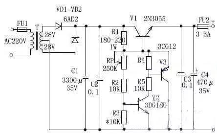
1. 3~25V Adjustable Voltage Regulator Circuit
The adjustable range of this regulated power supply can be adjusted arbitrarily between 3.5V and 25V, output current is large, and regulated voltage regulation circuit is used to obtain a satisfactory and stable output voltage.
Working principle: After rectifying and filtering, a constant voltage is applied through R1 to base of adjusting tube, so that adjusting tube turns on. When V1 is turned on, voltage passes through RP and R2 to make V2 turns on, and then V3 also turns on. voltage time of emitter and collector V1, V2 and V3 no longer change (its function is exactly same as that of zener diode). By adjusting RP, a stable output voltage can be obtained, and ratio of R1, RP, R2 and R3 determines the output voltage value of this circuit.
Selection of components: Transformer T has a power of 80-100W, input voltage is 220VAC, and output voltage is 28VAC with double winding. FU1 selects 1A and FU2 selects 3A~5A. VD1 and VD2 use 6A02. RP selects about 1W common potentiometer, resistance value is 250K~330K, C1 selects 3300UF/35V electrolytic capacitor, C2 and C3 select 0.1UF monolithic capacitor, and C4 selects 470UF/35V electrolytic capacitor. 180~220Ω/0.1W~1W, R2, R4, R5 select 10kΩ, 1/8W. V1 uses 2N3055, V2 uses 3DG180 or 2SC3953, V3 uses 3CG12 or 3CG80
2. Regulated Power Supply Diagram 10A3~15V
Whether it is computer maintenance or electronic manufacturing, it is inseparable from a regulated power supply. The following is a regulated power supply with continuously variable DC voltage from 3V to 15V. The maximum current can reach 10A. The circuit uses temperature compensation, TL431 standard voltage source high-precision integrated circuit improves voltage regulation accuracy. If there is no special requirement, it can basically correspond to normal maintenance and use. The diagram is shown in figure below.
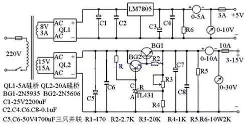
Its working principle is divided into two parts: first part is a 5V1.5A fixed regulated power circuit. The second part is another circuit of a high-precision, high-current, continuously adjustable voltage regulator from 3 to 15 V.
The first part of circuit is very simple. The DC voltage, rectified by secondary side of 8V AC transformer through QL1 silicon bridge, is filtered by electrolytic capacitor C1, and then LM7805 5V three-terminal voltage regulator can be output. without any adjustment. The terminal generates a fixed 5V1A regulated power supply, which can be used as an internal power source when repairing a computer board.
The second part is basically same as conventional series type regulated power supply, difference is that it uses high-precision integrated circuit of TL431 standard voltage supply with temperature compensation characteristics, so circuit is simplified, cost is reduced, and voltage stabilization performance is very high. . In figure, resistor R4, regulator tube TL431 and potentiometer R3 form a continuously adjustable constant voltage source, which provides a reference voltage for base of BG2. The voltage regulator value of regulator tube TL431 is continuously adjustable. The maximum output voltage of piezoelectric power supply. you can change resistance values of R4 and R3. Of course, secondary voltage of transformer must also be increased. The power of transformer can be flexibly adjusted according to output current, and secondary voltage is about 15V. The QL rectifier tube used for bridge rectification uses a 15-20A silicon bridge, which is compact in structure and has fixing screws in middle that can be fixed directly on case's aluminum plate to facilitate heat dissipation. The adjusting tube uses high-current NPN silicone tube with a metal case. Because it generates a lot of heat, if case allows, try to buy a large heatsink to expand heat dissipation area. smaller size. Use three 50V4700uF electrolytic capacitors C5 and C7 for filtering in parallel to make output large current more stable. In addition, this capacitor should be purchased with a relatively large volume. If it is not used for a long time, it will easily fail. Finally, let's talk about power transformer. If you do not have opportunity to wind it yourself, and there is no way to buy a ready-made one, then you can buy a ready-made switching power supply unit with a power of more than 200W to replace it. transformer. Thus, characteristics of voltage stabilizationi can be further improved, but cost of production is not much different. There are no special requirements for other electronic components, and they can work normally without much adjustment after installation.

Second
SwitchPower
1. The principle of operation of integrated control of PWM switching power supply IC-UC3842
How UC3842 works
The following figure shows internal block diagram and pinout of UC3842. The UC3842 uses a fixed operating frequency modulation mode with pulse width modulation. There are 8 contacts in total. The functions of each contact are as follows:
Pin ① is output terminal of error amplifier, and an external RC element is used to improve gain and frequency response of error amplifier;
Pin ② is feedback voltage input connector. The voltage on this pin is compared to 2.5V reference voltage of non-inverting pin of error amplifier to generate an error voltage for pulse width control;< /p>
Pin ③ is current detection input terminal. When detection voltage exceeds 1V, pulse width is reduced so that power supply is in an intermittent working state;
Pin ④ is timing terminal, internal oscillator operating frequency is determined by time constant of external resistance and capacitance, f=1.8/(RT×CT);
The icon ⑤ is public;
Pin ⑥ is a push-pull output connector, inside is a totem pole, rise and fall time is only 50ns, and drive power is ±1A;
Pin ⑦ is a DC power supply terminal that has an undervoltage and overvoltage blocking function, and chip power consumption is 15mW;
Pin ⑧ is a 5V reference voltage output terminal with a load capacity of 50mA.
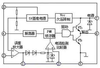
UC3842 Internal Block Diagram
UC3842 is an integrated PWM switching power supply controller with excellent performance, wide application and relatively simple structure. Since it has only one output terminal, it is mainly used for switching power supply controlled by tone terminal.
Pin 7 of UC3842 is a voltage input terminal, and its starting voltage range is 16V~34V. When power is on, Vcc﹤16V, Schmidt comparator output voltage input is 0, reference voltage is not generated at this time, and circuit is not works; when Vcc﹥16V, input voltage of Schmidt comparator sends a high level to 5V. As soon as Schmitt comparator switches to high level (after chip starts to work), Vcc can change in range of 10-34V without affecting operating state of circuit. When Vcc is below 10V, Schmitt comparator switches to low again and circuit stops working.
When voltage reference has an output reference of 5V, voltage reference detection logic comparator will output a high level signal to output circuit. At same time, oscillator will generate an oscillation signal f=/Rt.Ct according to Rt and Ct parameters externally connected to pin ④. One way of this signal is directly added to input end of totem pole circuit. , and other way is added to trigger RS of PWM pulse width system. The setting terminal, R terminal of RS type PWN pulse width modulator is connected to output terminal of current detection comparator. The R terminal is operation mode adjustment control terminal. When R voltage increases, Q terminal pulse expands, and at same time, width of pulse sent by ⑥ terminal also increases (duty ratio increases), when R terminal voltage drops, Q terminal pulse narrows. . At same time, width of pulse sent by pin ⑥ also becomes narrower (duty cycle is reduced). The figure shows time sequence of each point of UC3842. Only when point E is at a high level, there can be an output signal, and when points a and b are at a high level, then point d will send a high level, point c will send a low level, otherwise case d, point C will send a low level, and point C will send a high level. The ② pin is usually connected to output voltage sampling signal, also known as feedback signal. When voltage on pin ② increases, voltage on pin ① drops and voltage on pin R drops accordingly, so pulse on pin ⑥ becomes narrower, otherwise pulse on pine ⑥ becomes wider. ③ The pin is a current sensing terminal, and a small resistance sampling resistor is usually connected in series with source or emitter of power tube to convert current flowing through switching tube into a voltage and apply that voltage to pin. When load is short-circuited or other reasons cause current of power tube to increase and voltage of selection resistor exceeds 1V, terminal ⑥ stops pulse output, so that power tube can be effectively protected from damage.
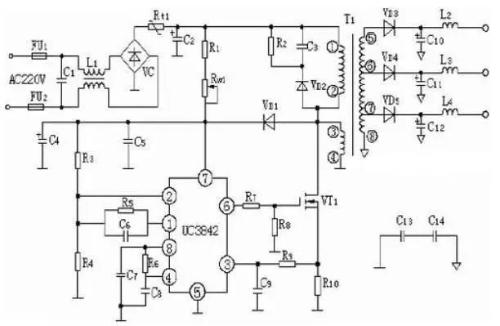
2. 12V, 20W switching regulated DC power supply, consisting of TOP224P
The figure shows a 12V, 20W regulated DC power supply switching circuit consisting of a TOP224P. The circuit uses two integrated circuits: a three-pin monolithic switching power supply TOR224P (IS1), a linear optocoupler RS817A (IS2). The AC source is rectified and filtered by UR and Cl to generate a high DC voltage Ui which energizes primary winding of high frequency transformer T. VDz1 and VD1 can limit peak voltage generated by leakage inductance to a safe value and attenuate ringing voltage. VDz1 uses a P6KE200 transient voltage limiter with a reverse breakdown voltage of 200V, and VDl uses a UF4005 1A/600V ultra-fast recovery diode. The secondary voltage is rectified and filtered by Vla, C2, Ll and C3 to obtain an output voltage Uo of 12 V. The value of Uo is given by sum of stable voltage Uz2 VDz2, forward voltage drop UF of LED in optocoupler and voltage drop across R1. Other output voltage values can also be obtained by changing transformation ratio of high-frequency transformer and value of stabilized voltage VDz2. R2 and VDz25 also provide preload for 12V output for better load regulation at light load. After feedback coil voltage is rectified and filtered by VD3 and C4, it provides bias voltage required by TOP224P. The control terminal current is regulated by resistors R2 and VDz2, and purpose of voltage regulation is achieved by changing duty cycle of output signal. The common mode choke L2 can reduce common mode leakage current generated by high voltage switching signal of primary winding connected to terminal D. C7 is a protective capacitor that is used to filter out interference caused by coupling capacitance of primary and secondary windings. C6 can reduce differential leakage current generated by fundamental and primary current harmonics. C5 can not only filter out peak current supplied to control terminal, but also detect self-start frequency, and compensate control loop together with R1 and R3.
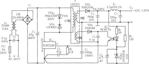
The main technical indicators of this power supply are as follows:
AC input voltage range: u=85~265V;
Input grid frequency: fLl=47~440Hz;
Output voltage (Io=1.67 A): Uo=12 V;
Maximum output current: IOM=1.67A;
Continuous output power: Po=20W (TA=25℃ or 15W (TA=50℃);
Voltage adjustment factor: η=78%;
Maximum output ripple voltage: ±60 mV;
Operating temperature range: TA=0~50℃.

Three,
DC-DCPower
1, wiring diagram 3V to +5V, +12V
Battery-powered portable electronic devices typically use a low power supply voltage, which reduces number of batteries and reduces size and weight of product. Therefore, 3~5V is usually used as operating voltage. To ensure stability of circuit and accuracy, it requires use of an adjustable power supply. If a circuit uses an operating voltage of 5 V, but a higher operating voltage is required, this often complicates designer's work. This article presents a two boost module circuit that can solve this problem and only needs two batteries to power it.
The circuit is characterized by fewer peripheral components, small size, light weight, stable +5V and +12V output, which meets requirements of portable electronic devices. The +5V power supply can output 60mA, and maximum output current of +12V power supply is 5mA.
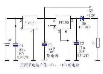
The circuit is shown in figure above. It consists of AH805 boost module and FP106 boost module. AH805 is a step-up module with 1.2-3V input and 5V output. It can output 100mA when powered by 3V. FP106 is an SMD boost module with 4-6V input, 29±1V fixed output and output current up to 40 mA. AH805 and FP106 are level-adjustable power-off control terminals.
3V output from two 1.5V alkaline batteries is input to AH805, and AH805 outputs +5V, one of which is used as 5V output and other is input to FP106 to generate 28-30V, which corresponds to output after stabilization by voltage regulator tube Voltage 12 V.
It can be seen from figure that by changing Zener tube voltage regulation value, different output voltages can be obtained, and use is very flexible. The ⑤ pin of FP106 is power off control terminal. When power is off, power consumption is almost zero. When ⑤ pin is high > 2.5V, power is turned on; when ⑤ pin is low < 0.4V, power is off. It can be controlled by circuit or manually. If no control is required, connect pin ⑤ to pin ⑧.
2. Use MC34063 to make circuit diagram from 3.6V to 9V
No payload:
Input: 3.65V, 18µA (equivalent to a 600mAh battery for more than three years)
With load:
Output: 9.88V, 50.2mA, Input: 3.65V, 186.7mA, 72% efficiency
How it works:
When there is no load, pin 6 of chip is de-energized and stops working. The 3.65V input current is only 18uA (equivalent to a 600mAh battery for more than three years)!
When there is a load (Q1 has current Ieb), EC 8550 pole turns on and IC is powered to operate.
The operation of IC is determined by presence of a load equivalent to a battery.
The use of voltage conversion IC ensures high efficiency and stable output!
This circuit can be upgraded for more power and can be used as a "4.2V to 5V mobile power supply without switch". You can use battery pack as a backup power source for your phone!
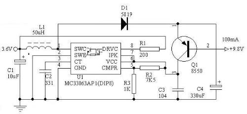
My inductor uses 0.3mm wire to wind about 30 turns on a 1cm I-shaped core. I think this core is too big and its space is not half wound.

Fourth
Charging circuit
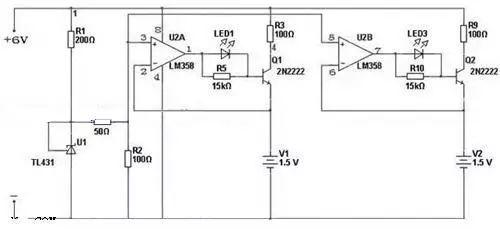
1. Alkaline Battery Charger Diagram lm358
There are two different opinions about whether alkaline batteries can be charged. Some say it can be charged and effect is very good. Some say that it cannot be charged, and instructions for battery indicate that there is a risk of explosion. In fact, alkaline batteries are indeed rechargeable and number of recharges is usually around 30-50 times.
Actually, there were two completely different consequences due to mastery of charge method. First, there is no doubt that alkaline batteries can be recharged, while at same time, instructions for batteries indicate that alkaline batteries are not rechargeable, and charging can lead to an explosion. This is also true, but note that wording here "may" cause an explosion. You can also understand this as a failure of manufacturer to protect itself. The key to charging alkaline batteries is temperature. As long as battery can be charged without high temperature, charging process can be completed smoothly. There are several requirements for correct charging method:
1. Small current 50mA
2. Charge only 1.7V, discharge 1.3V
After some people try to charge, they categorically say that it cannot be charged. The reason why there are problems such as failure to charge, low power consumption, liquid leakage, explosion, etc., basically a charger problem. , If charging current of charger is too high, much more than 50mA, for example, charging current of some fast chargers is higher than 200mA, direct consequence is that battery temperature is very high, it is hot to touch, it will leak. mild cases and it will explode in severe cases.
Some people use Ni-MH battery chargers for charging. Budget chargers do not have an automatic stop charging function. If battery is recharged for a long time, it will also leak and explode. The best charger has an automatic stop charge function, but charge stop voltage is usually set to 1.42V for Ni-MH rechargeable batteries, while full voltage of alkaline batteries is about 1.7V. Therefore, if voltage is too low, a impression that it can not be charged, and power consumption time is short, which does not affect. Another thing is that battery can not be discharged, which means that you do not need to wait for battery to be completely discharged before charging, so no matter how good battery is, it can be charged three to five times, effect is bad.
It is generally recommended to use Nanfu alkaline batteries with a voltage of at least 1.3V. Therefore, if you plan to charge alkaline batteries, you must have a qualified charger with a chargera current of about 50 mA and a charging cutoff voltage of about 1.7 V. Pay attention to a home charger.
There are special chargers for alkaline batteries on market, so-called proprietary products. In fact, this is a simple circuit with a charging voltage of 1.7V and a current of 50mA. Using LM358 and TL431 parts on hand, I made a simple circuit with a cutoff voltage of 1.67V to automatically stop charging, and cost is only two yuan. For reference of interested friends.
Instructions:
Alkaline manganese battery: Developed based on alkaline zinc manganese battery. Due to use of mercury-free zinc powder and new additives, it is also called mercury-free alkaline manganese battery. This type of battery can be charged and used tens to hundreds of times without changing discharge characteristics of original alkaline battery, which is more economical and affordable.
The alkaline zinc-manganese battery, known as alkaline manganese battery, was successfully developed in 1882, developed in 1912, and put into production in 1949. It has been found that by using KOH electrolyte solution instead of NH4Cl as electrolyte, both electrolyte and structure undergo great changes, and specific energy and discharge current of battery can be greatly improved.
Features:
1. The open circuit voltage is 1.5 V;
2. Wide operating temperature range is from -20°C to 60°C, suitable for use in alpine regions;
3. The high-current continuous discharge capacity is about 5 times that of zinc-manganese acid batteries;
4. Low temperature discharge is also very good.
The number of charging times is less than 30 times, usually 10-20 times, which requires a special charger, and it is very easy to lose ability to charge.
USB Charger Wiring Diagram Medium Power 2 2.75W
This design uses LNK613DG switch from Power Integrations' LinkSwitch family. This design is ideal for cell phones or similar USB chargers, including cell phone battery chargers, USB chargers, or any application that requires constant voltage/dc current characteristics.
In circuit, diodes D1-D4 rectify input AC current, while capacitors C1 and C2 filter DC current. L1, C1 and C2 form a π-type filter for differential mode conducted EMI suppression. Are these electronic transformer shields with Power Integrations? The combination of technologies allows this design to easily meet EN55022 Class B conducted EMI requirements with sufficient margin and without need for Y-capacitors. Flameproof Fused Wire Resistor RF1 provides protection against major faults and limits inrush current at start. V 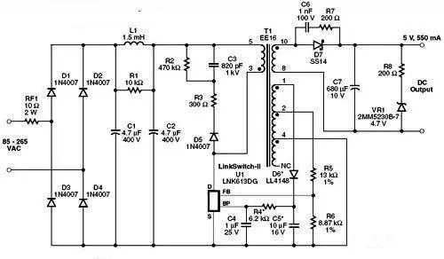
In fig. Figure 1 shows that U1 is powered by an additional bias supply, which reduces no-load power consumption to less than 40 mW. The value of shunt capacitor C4 determines amount of voltage drop compensation in cable. A value of 1 uF corresponds to compensation for a 0.3 ohm, 24 AWG USB output cable. (The 10 uF capacitor cancels out 0.49 ohm, 26 AWG USB output cable.)
In constant voltage stage, output voltage is controlled by switch. The output voltage is maintained by skipping switching cycles. Regulation can be maintained by adjusting ratio of on and off cycles. This also allows efficiency of converter to be optimized over entire load range. Under light load (drip charge) conditions, current limit is also lowered to reduce magnetic flux density of transformer, thereby reducing audible noise and switching losses. As load current increases, current limit will increase and fewer and fewer cycles will be skipped.
When no more switching cycles have been skipped (maximum power has been reached), controller in LinkSwitch-II will switch to DC mode. When load current needs to be increased, output voltage will drop accordingly. The drop in output voltage is reflected in voltage at FB pin. In response to voltage drop at FB terminal, switching frequency will decrease linearly, thereby achieving a constant output current.
D5, R2, R3 and C3 form an RCD-R termination circuit to limit drain voltage spikes caused by leakage inductance. Resistor R3 is relatively large in order to avoid drain voltage waveform fluctuation caused by leakage inductance, which can prevent excessive fluctuation during turn-off, thus reducing conducted electromagnetic interference.
Diode D7 rectifies secondary and C7 filters it. C6 and R7 work together to limit transient voltage peaks on D7 and reduce conducted and radiated EMI. Resistor R8 and Zener diode VR1 form an output preload that ensures output voltage without load is within acceptable limits and does not allow battery to completely discharge when charger is disconnected from AC mains. Feedback resistors R5 and R6 set maximum operating frequency and output voltage in DC voltage stage.

Five,
DC power
1. Talk about how to design a 3-wire DC power supply control
The DC power supply control circuitry is responsible for controlling Pt1000 temperature sensor and converting sensed resistance signal, which varies with temperature, into a measurable voltage signal. In this system, required DC power supply must have a constant output current, good temperature stability, large output resistance, output current less than 0.5mA (upper limit Pt1000 without self-heating effect), one end of load is grounded, and output current polarity can be adjusted, reversed characteristics.
Because influence of temperature on performance of integrated op amps is not as significant as that of transistors or FETs, a DC source consisting of integrated op amps has advantages of better stability and higher DC performance. It is widely used, especially when it is necessary to ground one end of load. Therefore, a DC power supply with two op-amps is used, as shown in Figure 2. Among them, UA1 is an adder and UA2 is a follower. no feedback.
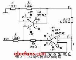
Assume that potentials of upper and lower poles of reference resistor Rref in Figure 2 are Va and Vb respectively, and Va is output of common mode adder UA1. With resistance R1=R2, R3=R4 , then Va=VREFx+Vb, Therefore, output current of a constant current source is:

You can see that DC power supply with two op-amps has following characteristics:
1) The load can be grounded;
2) When op-amp is powered by two power supplies, output current is bipolar;
3) Constant current is achieved by changing input reference reference VREF or adjusting size of reference resistor Rref0, and it is easy to obtain a stable low current and compensation calibration.
Due to resistor mismatch, voltage at both ends of reference resistor Rref0 will depend on voltage at Vb terminals of load it controls. At same time, since it is a constant current source, Vb is bound to change when load changes, which will affect stability of DC source. Obviously, this is unacceptable for high-precision DC sources. Therefore, principle of choosing four resistors R1, R2, R3 and R4 is that mismatch should be as small as possible, and mismatch size and direction of each pair of resistors should be constant. In practice, you can look at a large number of precision resistors from same lot to select 4 resistors with same resistance values.
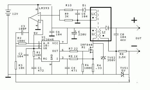
2. Switching power supply circuit with high withstand voltage and constant current
The development of device requires a constant current source that can generate a current of 1 mA with a resistance of 0 to 3 MΩ. One of them is based on UC3845 combined with 12V battery. About 24 turns of L3 uses original high voltage battery coil. voltage package, and L2 uses high voltage portion of high voltage package. L3 and LM393 form a voltage limiting circuit to prevent output voltage from being too high, and adjusting R10 can adjust open circuit output voltage.
Related
- A collection of basic schematic diagrams of power supplies, an indispensable book for engineers.
- The best switching circuit design process for power supplies is a must for engineers!
- A list of some of the tools commonly used by electronic engineers.
- Analysis of power circuit of a classic single-chip microcomputer
- Analysis of damping RC circuit of a switching power supply "haberdashery"
- Explain in detail classification of more than a dozen types of "recommended collection" capacitors
- Detailed analysis of the "various protection schemes" of a switching power supply
- Finally, it becomes clear that process of obtaining switching losses of a MOSFET in a switching power supply
- Perception of a ten-year-old workplace of an old electronics engineer
- The distribution parameters for magnetic components should be used by specialists in switching power supplies.
Hot Posts
 How to distinguish induction from leakage, we will teach you three tricks! Ordinary people can also learn super practical
- What is drowning in gold? Why Shen Jin?
- This is a metaphor for EMI/EMS/EMC that can be understood at a glance.
- How many types of pads have you seen in PCB design?
- Summary of Common PCB Repair Techniques
- What is three anti-paint? How to use it correctly?
- Knowing these rules, you will not get confused looking at circuit diagram.
- How to make anti-interference PCB design?
- Can diodes do this?