Location:Home Page > Archive Archive
Commonly Used Peripheral Diagrams, Hardware Design Reference and Precautions
2023-03-18【Archive】
Today, I would like to share with you some design diagrams and experience with small hardware circuits for reference of friends who are just learning about embedded systems. If there are any errors or omissions, you can correct them.
1. General guidelines for designing button circuits
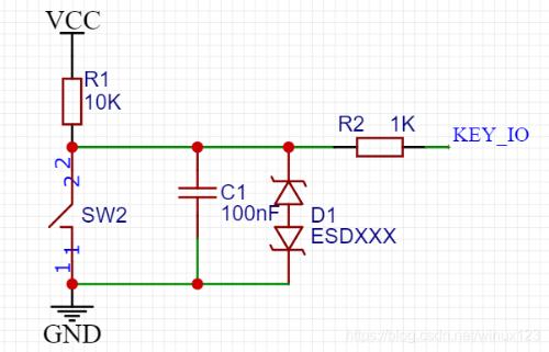
1. The pull-up resistor R1 latches undefined signal high across resistor and maintains non-triggered state or resets when triggered. (Private offer plus)
2. Capacitor C1 reduces button vibration and high frequency signal noise. (Private offer plus)
3. Current limiting resistor R2 (value ranges from 100 ohms to 10 k ohms. If there is an internal pull-up, value should not be too large, otherwise there will not be enough current to pull up I / O port) to protect I / O port from overcurrent and high voltage An I/O port burnout can absorb static electricity or some high voltage pulses. (Private offer plus)
4. Diode D1ESD Anti-static diode to prevent static interference or damage to I/O port. (It depends on cost of PCB and requirements for level of protection to decide whether to add or not)
2. External signal input design reference (similar to buttons)
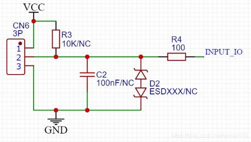
1.Pull-up resistor R3 Clamps an undefined signal high across resistor, holding it in unoperated state, or resetting it after being triggered. (If external trunk line is relatively long and internal pull-up capability of chip is relatively weak, it is recommended to add it. Generally, communication distance is short and internal pull-up can be omitted)
2. Capacitor C2 prevents high frequency signal interference. (Note, if input frequency signal is relatively large, capacitance of C2 must be reduced accordingly, or C2 can be omitted directly)
3. The current-limiting resistor R4 protects I/O port, prevents I/O port from burning due to overcurrent and high voltage, and absorbs static electricity or some high voltage pulses. (Private offer plus)
4. ESD diode D2ESD to prevent static interference or damage to I/O port. (It depends on cost of PCB and requirements for level of protection to decide whether to add or not)
Third, a link to output circuit relay design
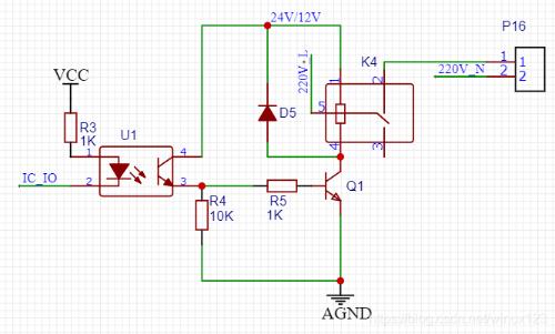
1. Optocoupler U1 separates high and low voltage to prevent high voltage interference and provide galvanic isolation
2. D5 1N4148 flyback diode protects component from induced voltage failure or burnout The circuit is drawn in form of DC current, thereby protecting components in circuit from damage.
Fourth Darlington Reference Design Application
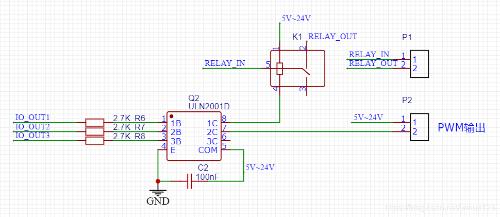
Darlington transistors are commonly used in stepper motor drives, but they can also be used to control speed of motors, high power switching circuits, drive relays, drive relatively high power LED lights, and use PWM for dimming.
1. Resistors R6 R7 R8 are used for current limiting to prevent damage to ULN2001, causing high voltage to be directly applied to I/O of MCU (because ULN2001D itself has a 2.7K resistor, R6 R7 R8 can be omitted here if some chips drivers are not suitable.It is best to add resistor yourself.For specific conditions, you can check data sheet of selected chip to make a decision)
2. The COM terminal is connected to power supply. When output terminal is connected to an inductive load, there is no need to add a freewheeling diode to load. The diode is designed inside chip. You only need to connect COM port to load power supply, you can skip it.
3. When using an RC buck circuit to supply power to ULN2001D, since an RC buck circuit cannot prevent transient high voltage fluctuations in mains, a 104 capacitor must be connected to COM terminal and ULN2001D ground terminal nearby. In some cases, capacitance may not be added.
5. Operational Amplifier Design Reference Application
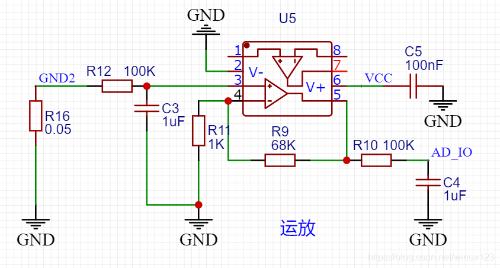
By using op-amp to intelligently collect current load current, you can know current working state of load accurately and whether it is working normally, which is very useful. There are many neat and practical op amp circuits, and I will share them with you one by one in future. If you have time, you can also search for some classic op amp circuits on Internet, and there are many for reference.
1. GND2 is load ground terminal. It is connected to common ground through resistor R16 (R16 should be selected with more power according to load current), and there will be a slight voltage difference< /p>
2. The circuit is a proportional action circuit with same phase, so voltage at sampling terminal = voltage at input terminal * (1+R9/R11) = 69 times input voltage. You can change R9 to adjust magnification according to measuring range.
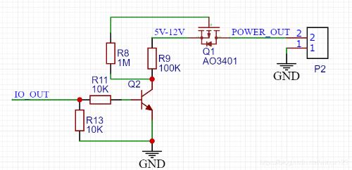
6. MOS tube design reference application (power output on and off)
7. Input Power Supply Design Reference Application
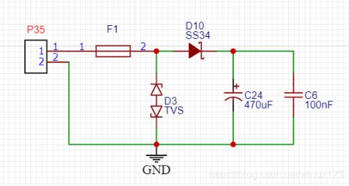
If circuit cost is relatively low, components can be removed as needed
1.F1 self-recovery fuse, overcurrent protection, threshold value can be adjusted according to actual load current.
2. The D10 Schottky diode reduces effect of rear stage power supply on front stage, prevents positive and negative power supply leads from burning out in last stage circuit, and prevents current from flowing back when power is turned off. However, a voltage drop of about 0.4V is observed through diode. Consideration should be given to whether it will be lower than normal operating voltage of downstream circuit after a 0.4V reduction.
3. The input voltage of TVS tube is too high, usually 1.4 times normal input voltage.
Related
- Commonly Used Peripheral Diagrams, Hardware Design Reference and Precautions
- Hardware Circuit Design Specification: A Very Good Reference to Hardware Design
- Super practical! The 10 Most Commonly Used Power Supply Design Formulas
- Hardware Collection: 50 Common Circuit Diagrams
- Analysis and comparison of 6 most commonly used DC power supply circuits
- How many of these free and easy to use circuit design programs have you used?
- 50 Common Hardware Design Patterns
- Countdown of 8 most commonly used diodes
- Commonly Used Diode Circuits Essential for Engineers
- List of commonly used circuits for zener diodes
Hot Posts
 How to distinguish induction from leakage, we will teach you three tricks! Ordinary people can also learn super practical
- What is drowning in gold? Why Shen Jin?
- This is a metaphor for EMI/EMS/EMC that can be understood at a glance.
- How many types of pads have you seen in PCB design?
- Summary of Common PCB Repair Techniques
- What is three anti-paint? How to use it correctly?
- Knowing these rules, you will not get confused looking at circuit diagram.
- How to make anti-interference PCB design?
- Can diodes do this?