Location:Home Page > Archive Archive
With these two schematics, PCB design is easy!
2023-03-18【Archive】
The power supply circuitry is an important part of an electronic device. The quality of power supply circuit directly affects performance of product.
Classification of power circuits
The power supply circuits of our electronic products mainly include linear power supply and high frequency switching power supply. In theory, a linear power supply determines how much current user needs and how much current is provided at input; The switching power supply determines how much power user needs and how much power is provided at input.
Linear Power Circuit Example
Linear power supply devices operate in a linear state, such as our commonly used voltage regulator ICs LM7805, LM317, SPX1117, etc. 1 below is LM7805 regulated power supply circuit diagram.
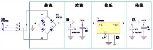
Figure 1. Schematic diagram of a linear power supply
As you can see from figure, linear power supply consists of functional components such as rectification, filtering, voltage stabilization and energy storage. At same time, conventional linear power supply is a series regulated power supply, and output current is equal to input current. I3 is reference end, current is very small, so I1≈I3. Why we are talking about current is because width of each line is not randomly set during PCB design, but is determined according to current size between component nodes on circuit diagram. The magnitude of current and direction of current must be clarified in order to make board just right.
Linear Power Supply PCB Schematic
When designing a printed circuit board, layout of components should be compact, and all connections should be as short as possible, and components and wiring should be arranged according to functional relationships of components on circuit diagram. . In this power supply circuit, rectification is performed first, then filtering, after filtering, voltage stabilizes, after voltage stabilizes, a storage capacitor flows through capacitor before power is used for subsequent circuits.
Figure 2 is circuit board diagram of above circuit, and two circuits are similar. The wiring on left and right is slightly different. The power supply in left figure is rectified and directly reaches input pin of voltage regulator chip, and then voltage regulator capacitor. The filtering effect of capacitor is much worse here. There are also problems with output. The picture on right is better. We need to not only consider flow direction of positive power supply, but also problem of ground return. Generally speaking, positive power line and ground return line should go in and out at same time as possible, and should be as close to each other as possible.
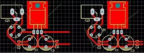
Fig. 2. PCB diagram of a linear power supply
When designing PCB of a linear power supply, you should also pay attention to heat dissipation of power regulator chip of linear power supply and how heat is generated. If input voltage of voltage regulator chip is 10V, output terminal is 5V, and output current 500 mA, then a voltage drop of 5 V occurs on voltage regulator chip, and heat generated is 2.5 W; if input voltage is 15V, voltage drop is 10V and heat generated is 5W. Provide enough space for heat dissipation or a reasonable heat sink. Linear power supply is generally used in applications where voltage difference is relatively small and current is relatively small, otherwise use a switching power supply circuit instead.
Example of high-frequency switching power supply circuit
The switching power supply must use switching tube driving circuit to carry out high-speed on and off, generate a PWM signal, pass through inductor and freewheeling diode, and use electromagnetic energy conversion method to adjust voltage. The switching power supply has high power, high efficiency and low heat generation. The circuits we usually use are LM2575, MC34063, SP6659, etc. The theory of switching power supply is that power at both ends of circuit is same, voltage is inversely proportional, and current is inversely proportional.
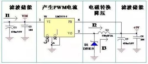
Figure 3. LM2575 Switching Power Supply Schematic
Scheme of printed circuit board of switching power supply
When designing circuit board of a switching power supply, following points must be considered: point of entry of feedback line and for whom shunt diode is intended. Figure 3 shows that when U1 is turned on, current I2 flows into inductor L1. The characteristic of inductor is that current cannot be formed or disappear suddenly when current flows through inductor. There is a time process for changing current in inductor. Under action of pulse current I2 flowing through inductor, part of electrical energy is converted into magnetic energy, and current gradually increases. At a certain point in time, control circuit U1 turns off I2. Due to nature of inductor, current cannot suddenly disappear. At this time, diode works Yes, it replaces current I2, so it is called a freewheeling diode. It can be seen that a freewheeling diode is used for inductance. The free current I3 starts at negative terminal of C3 and flows to positive terminal of C3 after passing through D1 and L1. This is equivalent to a water pump using energy of an inductor to increasing voltage of capacitor C3. There is also problem of introducing a voltage detection feedback line, it must be connected after filtering, otherwise output voltage ripple will be larger. These two points are often overlooked by many of our PCB designers, thinking that same network is not same where it is connected, but in reality connection is different and performance impact is great. Figure 4 is a circuit board diagram of LM2575 switching power supply. Let's see where wrong image is wrong.
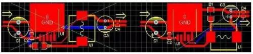
Fig. 4. Circuit board of switching power supply LM2575
Why we explain in detail concept of building a circuit diagram, since schematic diagram contains a lot of information about drawing a PCB, such as hotspot of component pins, current size of host, etc. By clearly seeing circuit diagram, PCB design will not be completed . The LM7805 and LM2575 circuits are typical layout diagrams of a linear power supply and a switching power supply, respectively. When making a PCB, you can directly follow layout and wiring of these two PCB diagrams, but products are different, and PCBs are also different. , Adjust according to actual situation.
Every change is same, so power supply circuit layout principle and method are same, and each electronic product is inseparable from power supply and its circuit. Therefore, after studying these two circuits, others are clear to chest.
Related
- With these two schematics, PCB design is easy!
- How many of these free and easy to use circuit design programs have you used?
- Switching Power Supply PCB Design Skills
- How to make anti-interference PCB design?
- PCB design guidelines: safety regulations, layout and wiring, EMC, thermal design, process engineering.
- Why PCB design usually controls 50 ohm impedance
- PCB puzzle, these few special rules!
- A Few Design Tips PCB Engineers Need to Know
- How many types of pads have you seen in PCB design?
- Do you know layout requirements of some special devices in PCB design?
Hot Posts
 How to distinguish induction from leakage, we will teach you three tricks! Ordinary people can also learn super practical
- What is drowning in gold? Why Shen Jin?
- This is a metaphor for EMI/EMS/EMC that can be understood at a glance.
- How many types of pads have you seen in PCB design?
- Summary of Common PCB Repair Techniques
- What is three anti-paint? How to use it correctly?
- Knowing these rules, you will not get confused looking at circuit diagram.
- How to make anti-interference PCB design?
- Can diodes do this?