Location:Home Page > Archive Archive
PCB design guidelines: safety regulations, layout and wiring, EMC, thermal design, process engineering.
2023-03-18【Archive】
Summary:
Safe Distance Requirements Section
Anti-interference protection, part of EMC
General layout and routing
Thermal Design Section
Processing part
Part 1
Safe Distance Requirements Section
Including electrical clearance (space distance), creepage distance (surface sliding distance), and insulation penetration distance.
1. Electrical clearance: The shortest distance, measured in air, between two adjacent conductors or a conductor and surface of an adjacent motor housing.
2. Creepage distance: The shortest distance between two adjacent conductors or a conductor and surface of an adjacent motor housing, measured along surface of insulation.
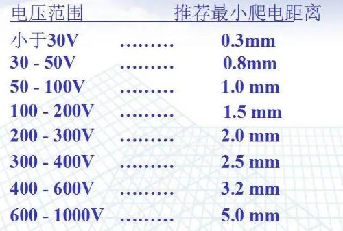
1. Creepage distance and clearance requirements:
1. Creepage distance: at input voltage 50-250V L-N in front of fuse ≥ 2.5mm, at input voltage 250-500V L-N before fuse ≥ 5.0mm, clearance : at input voltage 50-250V L-N before fuse ≥ 1.7mm, at input voltage 250-500V L-N before fuse ≥ 3.0mm, after fuse there is no requirement, but try to keep a certain distance to avoid short circuit damage to power supply;
2. Primary side AC to DC part ≥ 2.0mm;
3. Primary side DC ground to ground ≥ 4.0 mm, e.g. primary side ground to ground;
4. Distance from primary to secondary side ≥ 6.4mm, such as optocoupler, Y-capacitor and other components with pitch ≤ 6.4mm to be cut;
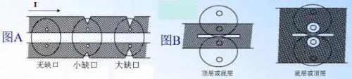
5. The distance between two stages of transformer is more than 6.4mm, and insulation is more than 8mm.
Part 2
Anti-interference protection, part of EMC
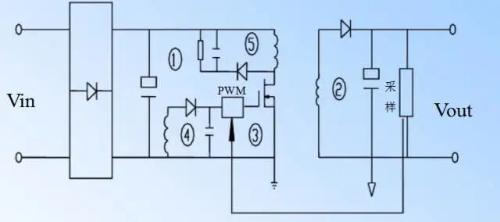
1. Long line interference protection
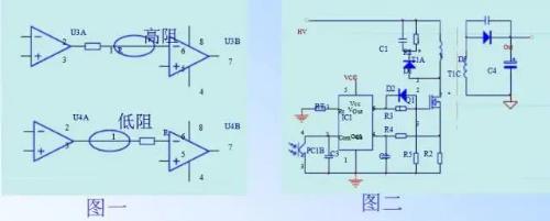
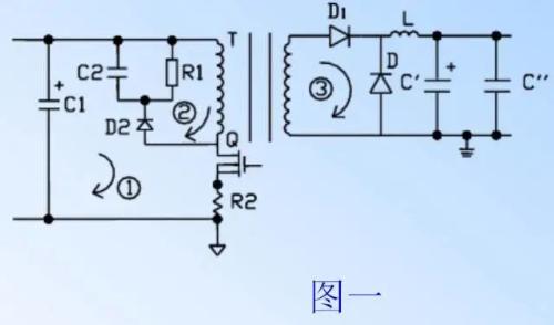
In figure 2, during PCB layout, control resistor R3 should be near Q1 (MOS lamp) and current sampling resistors R4 and C2 should be near 4th pin of IC1. As shown in Figure 1, R should be as close to op-amp as possible to shorten impedance line in height. Because input impedance of an op-amp is very high, it is susceptible to interference. The output impedance is low and not susceptible to interference. A long line is equivalent to a receiving antenna, which is easy to introduce external interference.
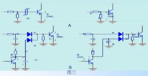
When typing in A in fig. 3 resistors R1 and R2 should be placed close to transistor Q1, because input resistance of transistor Q1 is very large, base line is too long and subject to interference, so resistors R1 and R2 R2 should not be far from Q1.
When dialing in B in fig. 3, C2 must be close to D2, because input impedance of Q2 triode is very large, if line from Q2 to D2 is too long, interference may easily occur, and C2 must move to D2 region.
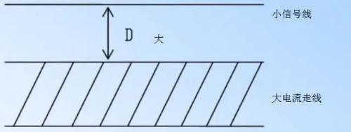
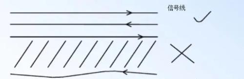
Secondly, weak signal traces should be as far away from high current traces as possible, avoid parallelism, D>=2.0 mm.
3. Small signal line processing: PCB wiring should be concentrated as much as possible to reduce layout area and improve noise immunity.
Fourthly, current loop tracing minimizes enclosed area.
Example: current sampling signal line and optocoupler signal line
5. Optocoupler devices easily interfere and should be kept away from devices with strong electric and magnetic fields such as large current circuits, transformers, devices with high ripple potential, etc.
6. Power supply for multiple ICs, pay attention to Vcc and ground wire.
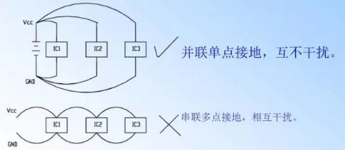 Serial multi-point grounding, mutual interference
Seven: noise requirements
1. Minimize area surrounded by high frequency pulse current as follows (Figure 1, Figure 2)
General layout method:
2. The filter capacitor should be as close as possible to switch lamp or rectifier diode. As shown in Figure 2 above, C1 should be as close to Q1 as possible, and C3 should be as close to D1 as possible.
3. The area where pulse current flows is far away from input and output terminals, so noise source is separated from the input and output ports.
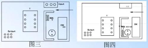
Figure 3: The MOS tube and transformer are too close to input, and EMI energy directly affects input end, so EMI test fails.
Figure 4: MOS lamps and transformers are far away from input, and distance between electric and magnetic radiation energy increases from input end, so they cannot directly affect input end, so conduction of electromagnetic interference can pass through.
4. The control circuit is separated from power circuit, and single-point grounding method is used, as shown in Figure 5.
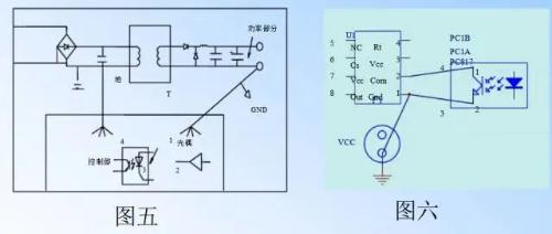
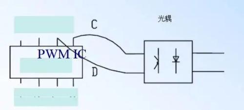
The ground of components around control IC is connected to ground pin of IC, then ground pin to ground wire of large capacitor. Connect pin 3 of optocoupler to pin 1 of IC and pin 4 to pin 2 of IC. As shown in Figure 6.
5. If necessary, output filter choke can be placed on ground loop.
6. Use multiple low ESR capacitors for parallel filtering.
7. Use copper foil for low inductance, low resistance wiring. There should not be too long parallel lines between adjacent lines. Try to avoid parallel lines and intersecting vertical lines. Do not drastically change line width. Angles (ie: ≤ right angles). (Parallel connection of same current loop can improve noise immunity)
Eight, anti-jamming requirements:
1. Shorten coupling between high-frequency components as much as possible and try to reduce their propagation parameters and mutual electromagnetic interference. Interference-prone components should not be too close to each other with strong interference devices, and input and output components should be as far apart as possible.
2. There may be a large potential difference between some components or wires, and distance between them should be increased to avoid an accidental short circuit caused by a discharge.
General layout and connection principles
1. General layout
1. The cooling fins are evenly distributed and air channel is well ventilated.
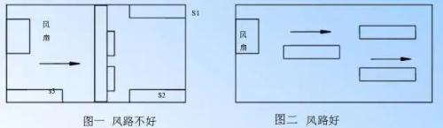
Fig. 1. The radiator blocks wind path, which does not contribute to heat dissipation.
Picture 2. Good ventilation, good heat dissipation
2. Capacitors, integrated circuits, etc. should be kept away from thermal components (heat sinks, rectifier bridges, freewheels, power resistors) so that they are not exposed to heat.
3. Current loop: For ease of threading, distance between wire holes should not be too large or too close.
4. The input/output and AC power/socket should be same length of two wires, leave a certain margin of space, pay attention to position occupied by plug buckle, easy to plug and unplug, neat wire hole exit, good welding wire.
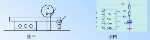
5. The components cannot touch each other, screw position of MOS tube and rectifier tube, and ball cannot touch other parts, so that assembly process can be simplified as much as possible. Capacitance and resistance may collide with bead or screw. Consider placement of screw and bead. As shown in Figure 3:
6. In addition to thermal switches and thermistors, key temperature-sensitive components (such as ICs) should be kept away from heating elements, and devices that generate a lot of heat should be kept away from capacitors and other devices that affect life of entire machine.
7. When placing adjustable components such as potentiometers, adjustable inductors, variable capacitors and microswitches, design requirements of entire machine should be taken into account. position must match position of adjustment knob on chassis panel.
8. The position occupied by PCB hole bracket must be reserved.
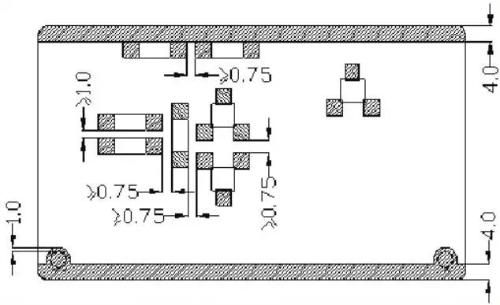
9. Components located at edge of PCB are typically at least 2mm from edge of PCB.
10. The output wires, lamp wires and fan wires should be as far apart as possible, and polarity should match panel.
11.General scheme: small board is not connected to high voltage, and high voltage components are placed on large board. Under special circumstances, safety regulations must be taken into account. As shown in Figure 4, place R1 and R2 on large board and enter low voltage line.
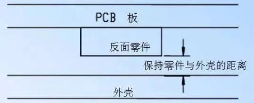
12. The distance between primary heatsink and case must be more than 5 mm (except for Mylar sheet).
13. When laying out board, pay attention to height of back components. Rice. 5:
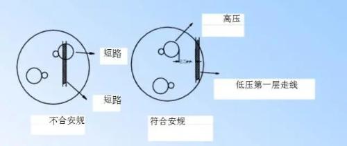
14. Pay attention to safety rules of primary and secondary Y capacitors and transformer cores.
Second,Device Schematic Layout Requirements
1. Arrange each functional unit of circuit according to flow of circuit, make layout convenient for signal flow, and keep signal in same direction as much as possible.
2. Take main components of each functional diagram by center and spread around it. Components should be placed on PCB evenly, neatly and compactly, and connecting wires between components should be minimized and shortened. as much as possible.
3. When working at high frequency, distribution parameters of components should be taken into account. In general circuits, components should be arranged as parallel as possible. Not only is it beautiful, but it is also easy to assemble and weld, and easy to mass-produce.
Third, connection principles
1. The wires used for input and output terminals should not be parallel to each other as much as possible, and it is better to add a ground wire between wires to avoid feedback.
2. The width of track is mainly determined by strength of bond between wire and insulating substrate and amount of current flowing through them. With a copper foil 50 µm thick and 1 mm wide, temperature rise will not exceed 3°C when a current of 1 A flows through it, so it is calculated that a 2 oz (70 µm) thick copper foil can flow 1.5 A current at a width of 1 mm, and temperature rise will be no more than 3°C (note: natural cooling).
3. The width of electrical gap between part of input control circuit and part of output current and control (that is, distance between small current tracks and output tracks) is: 0.75mm - 1.0mm (Min0.3mm) . The reason is that if copper foil and pad are too close, it is easy to cause a short circuit, and it is also easy to cause adverse electrical noise reactions.
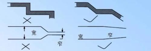
4. The angle of ROUTE line is usually arcuate, while a right angle and an acute angle will affect electrical performance in high frequency circuits.
5. According to magnitude of line current, width of power line should be thickened as much as possible to reduce loop resistance. At same time, direction of power line and ground line should be in line with direction of data transmission, reducing surrounding area and helping to improve anti-noise ability.
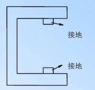
A: Most radiators are also grounded at one point to improve noise suppression capability, as shown in picture below:
Before change: The multi-point ground creates a magnetic field loop and EMI test fails.
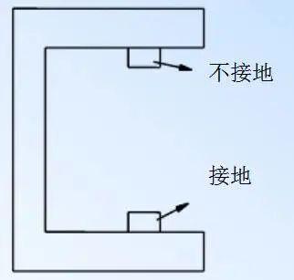
After change: single-point grounding without magnetic field loop, EMI test passed.
7. Filter Capacitor Wiring
A: Noise and ripple are completely filtered out by filter capacitor.
B: When ripple current is too high, several capacitors are connected in parallel and ripple current passes through first capacitor. When ripple current is too high, several capacitors are connected in parallel, and heat generated by ripple current passes through first capacitor. It is also larger than second and third and is easily damaged. When connecting, try to distribute ripple current to each capacitor equally. The wiring is shown in Figure A and B. If space permits, you can also use wiring shown in Figure B.
8. There is a rivet on contact of high voltage high frequency electrolytic capacitor, as shown in figure below, it must be kept away from copper foil on top layer, and must comply with safety requirements. regulations.
9. Low signal routing, do not route under devices such as inductors and current loops.
When current sampling line is mass-produced, magnetic core and copper foil of line collide resulting in failure.
10. Do not run high voltage line under metal film resistor, and low voltage line should be as close to middle of resistor as possible. If resistor is broken, it is easy to short circuit it. with copper wire at bottom.
11. Add tin:
A: Add tin to narrow part of power line copper foil;
B: RC absorption circuit not only requires addition of tin to increase current, but also promotes heat dissipation;
C: Add tin under fuser to dissipate heat, and tin can't press against pad.
12. Signal lines cannot pass through transformers, heatsinks, and MOS pins.
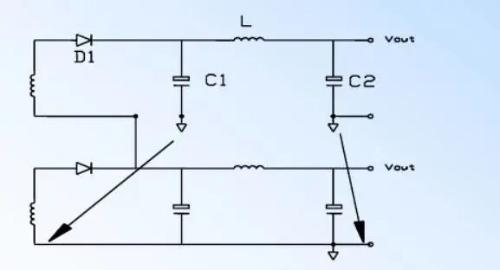
13. If output is superimposed, capacitor before differential mode inductor is connected to front end ground, and capacitor after differential mode inductor is connected to output ground.
14. High-frequency impulse current path area:
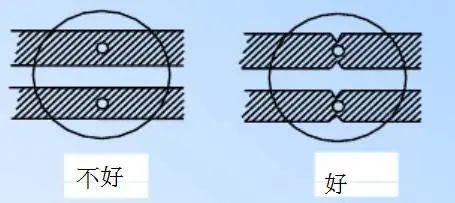
A: Minimize area surrounded by high-frequency pulse current. The area surrounded by five circuits marked in figure above should be as small as possible.
B: The power line and ground line should be as close as possible to reduce indoor area, thereby reducing electromagnetic interference caused by cutting external magnetic field loop, and at same time reduce external electromagnetic radiation. loops.
C: The large capacitor should be as close to MOS tube as possible, and absorption RC output circuit should be as close as possible to rectifier tube.
D: Power line and ground line wiring should be as thick and short as possible to reduce loop resistance.
E: The area where pulse current flows is far from input and output terminals, so noise source and output are separated.
F: The oscillation filter decoupling capacitor is located close to ground of IC, so ground wire must be short.

15. Manganin wire, vertical transformer, magnetic core, I-shaped inductance, power, resistance, heat sink, magnetic ring, can not pass through first layer of wires.
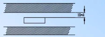
16. There must be a distance of more than 10 mils between groove and copper foil of wiring, and pay attention to safety rules of upper and lower metal parts.
17. Drive transformer, inductance and current loop terminals with same name must be matched.
18. Double-sided boards typically add more vias to high-current traces, and tin is added to vias to increase current carrying capacity.
19. In one panel, jumpers must not touch other components. If jumpers are connected to high voltage components, a certain safety distance must be maintained from low voltage components. At same time, keep more than 1mm away from heatsink.
The fourth analysis of situation
The volume of switching power supply is getting smaller and smaller, its operating frequency is getting higher and higher, and density of internal devices is getting higher and higher, which makes PCB wiring noise immunity requirements more and more stringent. . For some posting cases, following issues and solutions were found:
1. General layout
Option 1 - six-layer board. The first arrangement is to place control part on component side and power part on solder side. During debugging, it was found that there is a lot of interference. reason is that positions of PWM chip and optocoupler are unreasonable, for example:
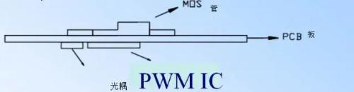
As shown in figure above, PWM chip and optocoupler are located under MOS tube, with only a 2.0mm PCB layer in between. The MOS tube directly interferes with PWM chip, and the improvement is as follows:
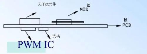
Remove PWM chip and optocoupler and there will be no ripple component above it.
2. Routing issue
The power bar should be as short as possible to reduce area surrounded by loop and avoid interference. The area surrounded by small signal lines is small, e.g. current loop:
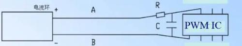
The larger area bounded by line A and line B, more interference it receives. Because larger area surrounded by feedback wire A and B, more interference it receives. Since this is a feedback coupler, feedback line must be short and there must be no pulsing signals crossing or paralleling it.
The current sampling lines of PWM chip and excitation lines, as well as synchronous signal lines, should be located as far apart as possible when wiring and should not be laid in parallel, otherwise they will interfere with each other. Current waveform:
PWM drive waveform and synchronous signal voltage waveform:
Part 4
Thermal design section
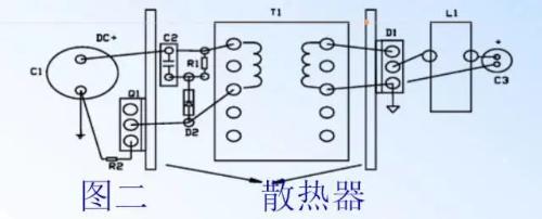
Note. The small plate should not be too close to transformer
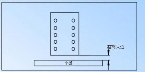
The small board is placed too close to transformer, which can cause semiconductor components on small board to become very hot.
Part 5
Processing Section
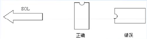
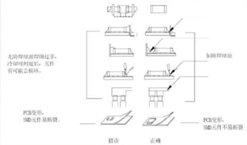
The direction of tin furnace should be marked with an arrow on each PCB:
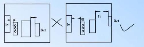
When laying out, placement direction of ICs in DIP packages should be perpendicular to direction of tin furnace, not parallel, as shown in figure below, if layout is difficult, it is allowed to place ICs horizontally (the direction of placement of ICs in SOP packages is same as in DIP).
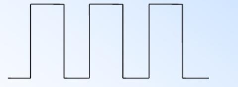
The direction of wiring is horizontal or vertical, and it takes 45 degrees to go from vertical to horizontal. If width of copper foil in round gasket is smaller than diameter of round gasket, droplets must be added. Wiring should be kept as short as possible, with particular attention to shorter wiring for sync lines, low level signal lines, and all high frequency loop wiring.
Ground wires and power systems for analog and digital circuits must be completely separated. If there are large areas of land and power lines on the printed circuit board (area exceeding 500 square millimeters), windows should be opened locally. As shown below:
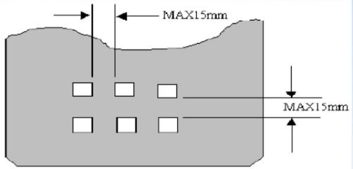
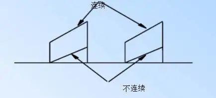
Lead spacing of horizontally inserted components (resistors, diodes, etc.) must be 300 mils, 400 mils, and 500 mils. (If not needed, 240 mils can also be used, but it is used on IN4148 type diodes or 1/16W resistors. 1/4W resistors start at 10.0mm) Jumper center spacing should be 200mil, 300mil, 500 mil, 600mil, 700mil, 800mil, 900mil, 1000mil The diameter of heat dissipation hole on printed circuit board must not exceed 140 mils.
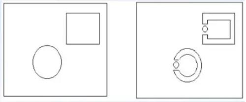
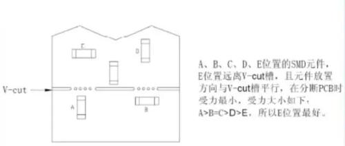
If PCB has a hole larger than Φ12 or a 12mm square, it is necessary to make a hole cover to prevent solder from flowing out, as shown in the figure below (1.0mm hole)
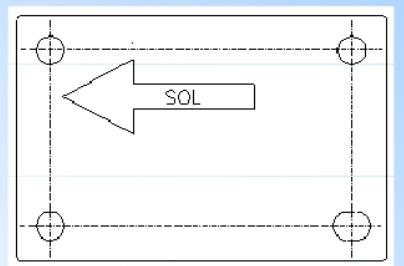
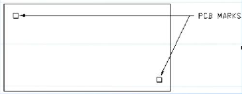
To improve accuracy of mounting SMD components on a printed circuit board, calibration marks (MARKS) must be applied to printed circuit board, and each board must have at least two marks, which are respectively installed on printed circuit board. diagonal corners as shown in picture below:
Patch Component Space:
The distance between SMD component and pin of pluggable electrical component. As shown in following two pictures:
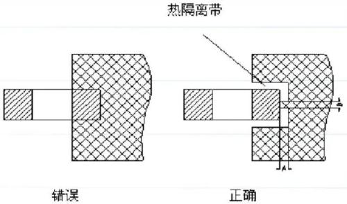
When terminals of SMD devices are connected to a large area copper foil, thermal insulation treatment is required, as shown in figure below:
The center hole of component's pad is slightly larger than device's pin diameter. If pad is too large, it will easily form a virtual connection. External pad diameter D is usually not less than (d +1.2) mm, d is pin aperture For high density increase accordingly. Components should be placed as neatly and in same direction as possible.
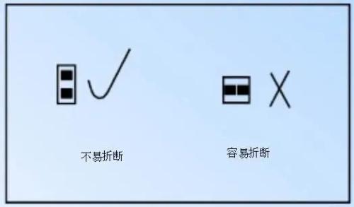
Try to position long axis of patch component on PCB in a direction perpendicular to long axis of PCB so that it is not easily broken.
Related
- PCB design guidelines: safety regulations, layout and wiring, EMC, thermal design, process engineering.
- Diagram of relationship between PCB layout and EMC
- Do you know layout requirements of some special devices in PCB design?
- Senior EMC Engineer Resume: EMC Troubleshooting Process and Common Problems
- What does inside of a multilayer PCB look like? Three-dimensional general analysis of design process of high-quality printed circuit boards
- Switching Power Supply PCB Design Skills
- How to make anti-interference PCB design?
- Power Knowledge - Flyback Transformer Design Process
- With these two schematics, PCB design is easy!
- Why PCB design usually controls 50 ohm impedance
Hot Posts
 How to distinguish induction from leakage, we will teach you three tricks! Ordinary people can also learn super practical
- What is drowning in gold? Why Shen Jin?
- This is a metaphor for EMI/EMS/EMC that can be understood at a glance.
- How many types of pads have you seen in PCB design?
- Summary of Common PCB Repair Techniques
- What is three anti-paint? How to use it correctly?
- Knowing these rules, you will not get confused looking at circuit diagram.
- How to make anti-interference PCB design?
- Can diodes do this?