Location:Home Page > Archive Archive
PCB puzzle, these few special rules!
2023-03-18【Archive】
Unified board refers to small printed circuit boards that are directly assembled by manufacturer into a single unit.
1. Why do you need to make boards, that is, what are advantages of making boards?
1. In order to meet needs of production. Some circuit boards are too small to fit fixture making requirements and must be assembled for production.
2. Improve efficiency of SMT patch welding. Only one SMT is required to complete welding of multiple PCBs.
3. Optimize use of costs. Some PCBs are specially shaped, and jigsaw boards can make better use of PCB area, reduce waste, and improve cost utilization.
Secondly, what are ways to create puzzles?
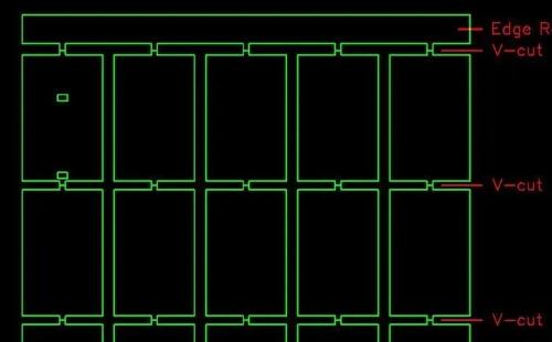
1. V-CUT
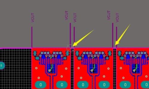
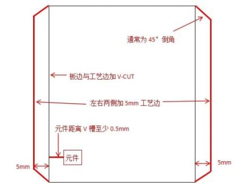
V-CUT is to draw a groove at junction of two boards, as long as two boards are joined together, there is a gap between them (usually 0.4 mm), but joint of boards at this point is relatively thin, it is easy to break, and edges of two boards must be joined together when assembling board.
V-CUT is generally a straight line, there won't be complex tracing like curved arcs, and try to be on a straight line when making boards.
2. Stamp Hole
For irregularly shaped PCBs, such as round ones, V-CUT cannot do this. Currently, die holes must be used to connect boards, so die holes are commonly used in specially shaped boards.
The edge of two boards is connected by a small board, and there are many small holes in joint between this small board and two boards, so it is easy to break. After being torn off, edge of board is like edge of a die, which is why this type of puzzle is called a die hole.
3. Hollow connection bar
Half-hole boards often use hollow connector strips. They are connected by very narrow plates, somewhat like stamped holes. The difference is that connecting part of connector strip is narrower and there are no holes on either side.
There is a drawback to jigsaw method of hollow tie bar: after board breaks, there will be a clear protrusion. The die holes also have ridges that are not as obvious as they are separated by vias.
Some people might think it's not enough to use die holes directly, why use hollow connector bars? This is because when manufacturing a module with all-round half-holes, neither punch hole nor V-CUT can be used, and they can only be connected at four corners of module using hollow connecting strips.
3. What is principle of puzzle?
For ease of production, try to keep slabs square after sheathing. In short, don't let aspect ratio gap be too big.
Fourth, indentation requirements:
2. Leave a gap of >0.5mm between components and V-CUT to ensure proper tool operation.
Related
- PCB puzzle, these few special rules!
- In PCB industry, we all need to know these 5 important common sense rules.
- A Few Design Tips PCB Engineers Need to Know
- Do you know layout requirements of some special devices in PCB design?
- With these two schematics, PCB design is easy!
- Knowing these rules, you will not get confused looking at circuit diagram.
- Should PCB trace angle be 90°? — Jumping guide to PCB layout pit
- General PCB debugging skills
- Pay attention to PCB vias
- Summary of Common PCB Repair Techniques
Hot Posts
 How to distinguish induction from leakage, we will teach you three tricks! Ordinary people can also learn super practical
- What is drowning in gold? Why Shen Jin?
- This is a metaphor for EMI/EMS/EMC that can be understood at a glance.
- How many types of pads have you seen in PCB design?
- Summary of Common PCB Repair Techniques
- What is three anti-paint? How to use it correctly?
- Knowing these rules, you will not get confused looking at circuit diagram.
- How to make anti-interference PCB design?
- Can diodes do this?