Location:Home Page > Archive Archive
Why can't crystal oscillator be placed on edge of the PCB?
2023-03-18【Archive】
01
Problem description
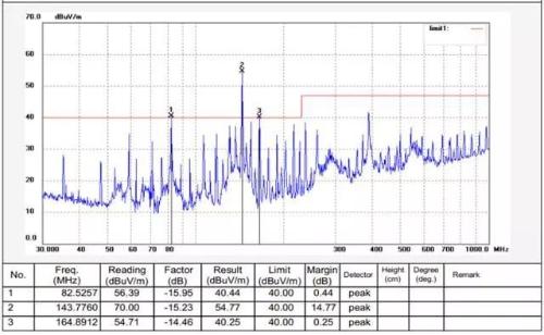
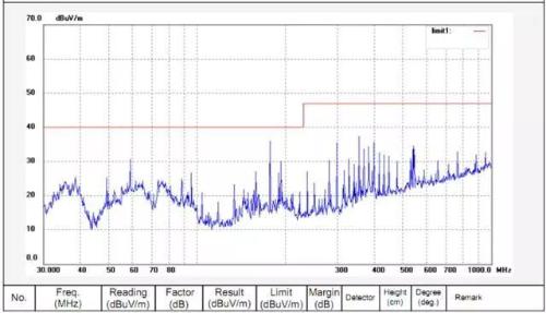
For driving recorder, you need to add an external adapter during test, and it was found to exceed standard when car is turned on and tested.
Radiation test data is as follows:
02
Emission source analysis
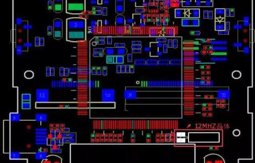
This product has only one PCB with 12MHz crystal.
Among them, over-standard frequency point is 12MHz multiplier, and analysis of screen and camera, which are subject to electromagnetic radiation exceeding standard of this machine, shows that LCD-CLK is 33MHz, and camera's MCLK is 24MHz.
Through exclusion, it is found that after removing camera, superstandard point still exists, and by shielding 12MZH crystal, superstandard point is reduced, so 144MHz superstandard point is considered to belong to chip, and PCB layout is as follows:
03
Principle of radiation generation
You can see from PCB layout that 12MHz die is simply placed on edge of PCB. When product is placed in a test environment with radiation, high-speed device of product under test and reference ground in laboratory will form a certain capacitance. Communication generates parasitic capacitance, resulting in common mode radiation. The larger parasitic capacitance, stronger common mode radiation.
The essence of parasitic capacitance lies in distribution of electric field between crystal and reference ground. When voltage between them is constant, greater distribution of electric field between them, greater electric field strength between them, and parasitic capacitance. The larger size of crystal, distribution of electric field when crystal is on edge of printed circuit board and in middle of printed circuit board looks like this:
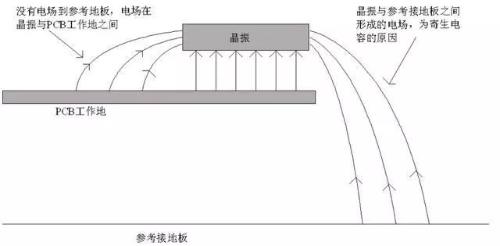
▲ Schematic diagram of distribution of electric field between crystal oscillator at edge of PCB and reference ground plane
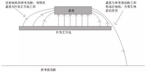
▲Electric field distribution diagram between crystal oscillator in middle of PCB and reference ground plane
It can be seen from figure that when crystal oscillator is located in middle of PCB or far from edge of PUB, due to presence of a working ground plane (GND) on PCB, most of electric field is controlled between crystal oscillator and working ground, that is inside printed circuit board, electric field distributed over reference ground plane is greatly reduced, resulting in reduced radiated noise.
04
Remedy
Move crystal oscillator inward so that it is at least 1 cm away from edge of PCB, and apply copper to surface of PCB within 1 cm of crystal oscillator, and bond copper on surface layer to PCB. ground plane through through holes.
The spectrogram of modified test results is as follows: figure shows that emitted radiation has improved significantly.
05
Thinking and enlightenment
High-speed printed lines or capacitive coupling between devices and reference ground plane will cause EMI problems, and sensitive printed lines or devices placed on edge of PCB will cause immunity problems.
If design needs to be placed on edge of PCB for other reasons, then work ground wire can be placed on edge of printed line, and extra vias are added to connect work ground wire to work wire. ground plane.
Related
- Why can't crystal oscillator be placed on edge of the PCB?
- Case analysis! Why can't crystal oscillator be placed on edge of PCB?
- What determines frequency of a crystal oscillator?
- Why can't copper and aluminum wires be twisted together when wiring?
- Daniel's Summary: The details and experience of 30 PCB layouts are wonderful.
- Should PCB trace angle be 90°? — Jumping guide to PCB layout pit
- Why PCB design usually controls 50 ohm impedance
- Can a PCB trace angle be 90 degrees?
- Summary of Common PCB Repair Techniques
- Hear how engineers talk about various "fantasies" about first power-up on PCB.
Hot Posts
 How to distinguish induction from leakage, we will teach you three tricks! Ordinary people can also learn super practical
- What is drowning in gold? Why Shen Jin?
- This is a metaphor for EMI/EMS/EMC that can be understood at a glance.
- How many types of pads have you seen in PCB design?
- Summary of Common PCB Repair Techniques
- What is three anti-paint? How to use it correctly?
- Knowing these rules, you will not get confused looking at circuit diagram.
- How to make anti-interference PCB design?
- Can diodes do this?