Location:Home Page > Archive Archive
USB trace layout experience, a painful lesson
2023-03-25【Archive】
USB is a fast, two-way, synchronous, low-cost, easy-to-use, hot-swappable serial interface.
Because of advantages of fast data transfer, user-friendly interface, and hot plug support, USB devices are widely used. Currently, most of products on market use USB 2.0 as an interface, but many newcomers to equipment encounter many problems when working with USB.Various problems often occur with USB interface after PCB assembly. .
For example, if connection is unstable or cannot communicate, check circuit diagram and soldering and there is no problem. Perhaps at this time one should suspect that PCB design is unreasonable.
A PCB drawing that meets USB 2.0 data transfer requirements is extremely important to product performance and reliability.
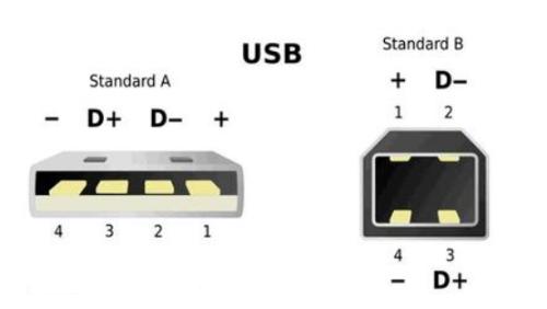
The USB protocol defines two differential signal lines (D+, D-) for transmission of digital signals. If you want a USB device to work stably on differential signal lines, you must strictly follow differential signal wiring rules. and wiring.
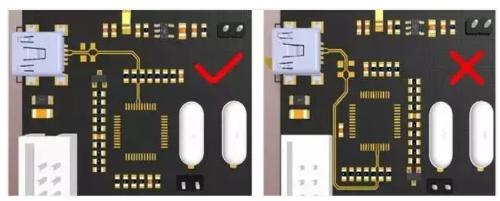
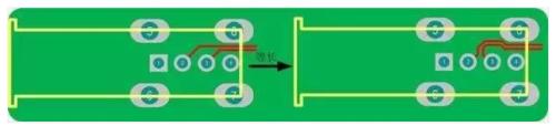
According to author's years of experience in designing and debugging USB related products, following points are summarized:1. When laying out components, try to make differential line as short as possible to reduce distance of differential line (√ is a reasonable path, × means an unreasonable path).
 2. Give priority to drawing differential lines. Try not to exceed two pairs of vias on a pair of differential lines (vias increase parasitic inductance of line, thereby affecting signal integrity of line). and they need to be arranged symmetrically (√ is a reasonable way, × is an unreasonable way).

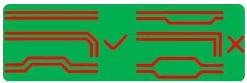
3. Symmetrical parallel routing that provides a tight connection between two wires and avoids 90° routing. The best routing methods are arc or 45° angle (√ is a reasonable way, × is an unreasonable way) .
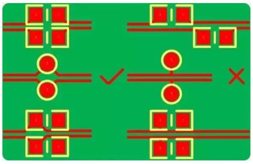
4. Placement of differential series resistors, test points, pull-up and pull-up resistors (√ reasonable, × not practical).
 5. Due to factors such as pin spacing, vias, and routing space, it is easy for differential line lengths to mismatch, and if line lengths do not match, timing shifts and common mode noise occurs. , degrading signal quality.
So, accordingly, compensation for mismatch of differential pair must be made so that lengths of lines match. The length difference is usually controlled within 5mil. The principle of compensation is where difference in length occurs.
 6. To reduce crosstalk, if space permits, distance between other signal networks and ground should be at least 20 mils from differential line (20 mils is an empirical value), and distance between ground and differential line is too close Line impedance has an effect.
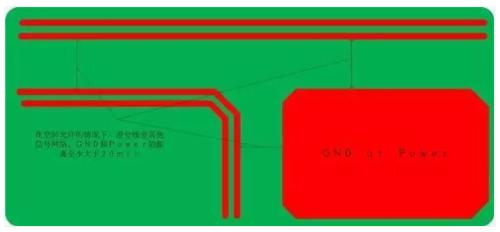 7. USB output current is 500 mA. Pay attention to width of VBUS and GND lines. If 1 oz copper foil is used, line width exceeds 20 mils to meet current requirements. Of course, larger line width, better integrity of power supply. good.
The signal line width and line spacing of differential line of conventional USB devices must match signal line width and line spacing of entire board.
However, when operating speed of USB device is 480 Mbps, it is not enough to follow only above steps. We need to control impedance of differential signal in order to control impedance pair of differential signal line The integrity of high speed digital signals is very important.
Because differential impedance affects eye diagram, signal bandwidth, signal jitter, and interference voltage on differential signal signal line.
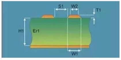
Line differential resistance is typically maintained at 90 (±10%) ohms (refer to chip manual for specific values). The line differential resistance is inversely proportional to line width W1, W2 and T1, inversely proportional to dielectric constant Er1, and inversely proportional to distance between lines. S1 is proportional to distance H1 to reference layer. The following figure shows cross section of differential line.
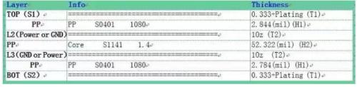
The figure below shows a reference stack of a four-layer board. The two middle layers are reference layers. The reference layer is usually GND or Power, and reference layer corresponding to differential line must be full and cannot be split, otherwise differential line will be damaged.
If a four-layer board is assembled and constructed as shown in figure below, differential line will typically have a line width of 4.5 mils and a line spacing of 5.5 mils to match a differential impedance of 90 ohms.
However, 4.5 mil line width and 5.5 mil line spacing are only our calculated values. impedance value and combined with actual production situation and board. Appropriate adjustments.
The connection rules described above are based on USB 2.0 devices. In USB connection process, use shortest differential lines, tight connection, same length, constant impedance, and pay attention to current carrying capacity. USB power line, master above principles, operation of USB devices is basically no problem.
Related
- USB trace layout experience, a painful lesson
- Should PCB trace angle be 90°? — Jumping guide to PCB layout pit
- Can a PCB trace angle be 90 degrees?
- Diagram of relationship between PCB layout and EMC
- Common USB Interface Circuit Design Problems and Solutions
- Frequently Asked Questions for USB Interface Circuit Design
- TVS choice, this experience is comfortable
- Do you know layout requirements of some special devices in PCB design?
- PCB design guidelines: safety regulations, layout and wiring, EMC, thermal design, process engineering.
- Daniel's Summary: The details and experience of 30 PCB layouts are wonderful.
Hot Posts
 How to distinguish induction from leakage, we will teach you three tricks! Ordinary people can also learn super practical
- What is drowning in gold? Why Shen Jin?
- This is a metaphor for EMI/EMS/EMC that can be understood at a glance.
- How many types of pads have you seen in PCB design?
- Summary of Common PCB Repair Techniques
- What is three anti-paint? How to use it correctly?
- Knowing these rules, you will not get confused looking at circuit diagram.
- How to make anti-interference PCB design?
- Can diodes do this?