Location:Home Page > Archive Archive
Should PCB trace angle be 90°? — Jumping guide to PCB layout pit
2023-04-18【Archive】
Now, whenever you open PCB layout guide of original SoC factory, you will always indicate corner angle of high-speed signal trace and say that high-speed signal should not be traced at a right angle, but at a 45 degree angle, rounded arc was would be better than a 45 degree angle. This is true? How to set PCB layout angle, which is better: 45 degrees or an arc of a circle? Is 90 degree right angle wiring suitable? This is a hot topic that I often see in most PCB layout bacteria.
Everyone has started getting tangled up in corners of PCB wiring, which has happened in last ten or twenty years. In early 1990s, Intel, master of PC industry, adopted PCI bus technology. It seems that, starting with PCI interface, we have entered era of "high-speed" system design. After 1990s, a group of players such as Lao Wu's pursuit of 3D performance allowed development of related electronic design and chip manufacturing technology in accordance with Moore's law. With continuous improvement of IC manufacturing process, switching speed of IC transistors is also getting faster. The bus clock speed is getting faster and faster, and problem of signal integrity is constantly attracting everyone's attention and research. For example, now people's demand for 4K HD home audiovisual video with standard HDMI2.0 bit rate has reached 18Gbps! ! !
Before I was born, pcb pull wire bacteria should be relatively simple classmates, just draw lines, smooth, clean and beautiful, and they don't need to pay attention to various signal integrity problems. For example, PCB of classic HP3456A six and a half digit multimeter shown in figure below shows a large number of 90° traces.
The HP3456A is almost right-angled intentionally (in some places it should go at a beveled angle, but it should go right-angled a few times in a row), and most of places aren't copper plated.
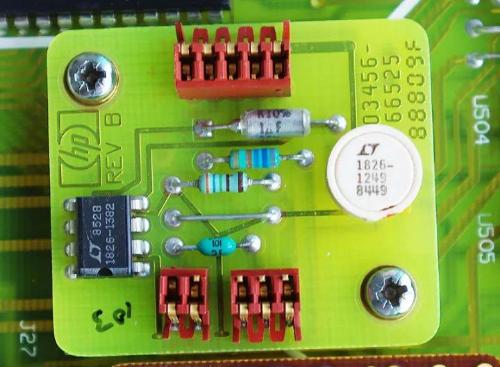
In upper right corner, angle is larger than right one, but line width has become smaller?
Right angles, jumpers, and copper wire routing - can simulation really fail to lay copper wires?
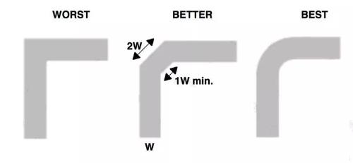
Right angle, 45 degree slash, any angle slash, square and round pads.
Can't high speed signal line be rotated 90°? Here to discuss corner angle of high frequency/high speed signal with you. Let's trace path from sharp corners to right angles, obtuse angles, arcs to arbitrary angles, and look at advantages and disadvantages of different milling angles.
Can I trace a PCB at a sharp angle?
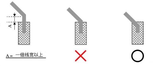
Whether it is possible to trace PCB at a sharp angle, answer is no, regardless of whether trace at a sharp angle will have a negative impact on high-speed signal transmission line, from point of view of DFM of PCB, situation of cutting at a sharp angle should be avoided.
Because PCB wires cross to form an acute angle, a problem called "acid traps" occurs. Excessive amount will break PCB line. While we can use CAM 350 to perform a DFF audit to automatically detect potential "acid trap" issues to avoid processing bottlenecks in PCB manufacturing. If PCB factory technicians detect acid traps, they will simply insert a piece of copper into this gap. Many engineers in board factory do not understand layout. They simply fix acid trap problem from PCB engineering point of view, but this repair will not cause problems. It is not known if it will cause further signal integrity problems, so one should try to avoid acid traps from source when laying out.
How to avoid sharp corners when pulling wires that cause problems with DFM acid trap? Modern EDA design software (such as Cadence Allegro, Altium Designer, etc.) has a complete Layout routing option. When we route a layout, we can use these auxiliary options flexibly to avoid "acid trap" phenomenon.
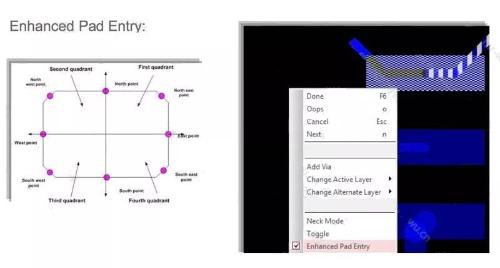
Setting exit angle of pad Avoid sharp corners between wire and pad.
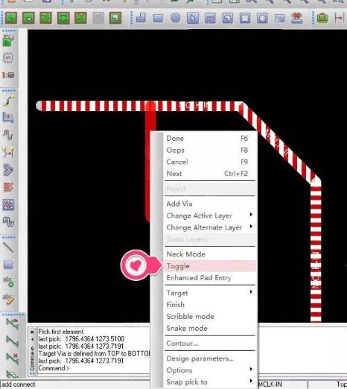
Using Enhanced Pad Entry feature in Cadence Allegro avoids angle between wire and pad as it exits during linking and avoids DFM problems associated with "acid traps".
Avoid sharp corners between two crossing wires.
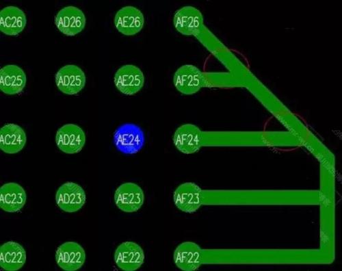
The flexible use of Cadence Allegro to toggle "tumbler" option during routing avoids sharp corners when pulling wire from a T-branch, and also avoids problem of DFM "acid traps".
PCB SchematicCan I wire at 90°
High frequency and high speed transmission lines should not be laid at 90° angles. At corner of transmission line, line width will be changed. The line width at 90° is about 1.414 times line width. Normal line width. As line width changes, it will cause signal to be reflected. At same time, extra parasitic capacitance in corner will also affect signal. Transmission causes delay effects.
Of course, when signal propagates along common connection line, there will be no reflection and distortion of transmitted signal. If there is a 90° angle on common connection line, it will cause PCB transmission to change. width of line at corner, calculated according to relevant electromagnetic theory, will necessarily result in a reflection of signal.
That's true in theory, but a theory is a theory after all. How important is effect of 90° angle on a high-speed signal transmission line in a real situation?
So, a 90° angle will have a negative effect on a high-speed signal transmission line, which is theoretically certain, but is this effect fatal? Does a 90° angle have same effect on high speed digital and high frequency microwave transmission lines?
According to this article "Right Corners on PCB Traces, Time and Frequency Domain Analysis" and this article "Who's Afraid of a Big Bad Bend?" Howard Johnson and Eric Bogatin's book "Signal Integrity" and based on contents of Chapter 8 of Power Integrity Analysis (Second Edition), we can draw following conclusions:
For high speed digital signals, 90° angle will have some effect on high speed signal transmission line. The capacitance of a 90° angle is about 10 fF, according to calculations, total delay caused by this capacitor is about 0.25 ps, so a 90° angle on a 5 mil wide wire will not have much effect on current high speed speed. digital signal (rise time 100 ps).
For high frequency signal transmission lines, in order to avoid signal damage caused by skin effect, a wider signal transmission line is generally used, such as 50 ohm impedance, 100 mil line width, line at 90° angle. The width is about 141 mils, and signal delay caused by parasitic capacitance is about 25 ps. At this time, 90° angle will have a very serious impact. At same time, microwave transmission line always hopes to reduce signal loss as much as possible. Impedance non-uniformity at 90° angle and external parasitic capacitance will cause phase and amplitude error of high-frequency signal, mismatch between input and output, and possible presence of parasitic coupling, will degrade circuit performance and affect PCB circuit signal transmission characteristics.
For signal routing at 90°, try to avoid routing at an angle90°, since one 90° angle will affect signal quality of high speed digital transmission line with respect to deviation of wire height and reference. flatness, linewidth of wire itself during etching process. The deviation of line spacing uniformity, change in board permittivity to frequency signal, and even influence of parasitic parameters of vias are much greater than problems caused by 90° angle. However, modern high-speed digital circuit transmission lines must inevitably be of uniform length, and with more than ten or twenty angles, rise time delay caused by cumulative effect of these 90-degree angles becomes significant. High speed signals are always carried along path with lowest impedance, with same length around 90° angles, and final actual signal path will be slightly shorter than original.
And current high-speed digital signal transmission rate is getting higher and higher. The current standard is HDMI 2.0, transfer rate reaches 18 Gbps, and 90° routing is no longer compliant, and now it's 21st century. Yes, current EDA software, even freeware, already supports 45° wiring very well.
At same time, 90° wiring does not match aesthetics of humans in terms of engineering aesthetics. Therefore, for current circuit, whether you use high frequency/high speed signal lines or not, we should try to avoid laying lines at 90° angles unless there are special requirements. For high-current traces, sometimes we replace traces with copper-plated copper skins. At corners of copper gasket, it is also necessary to replace 90° corners with two 45° corners, which is not only beautiful, but also has no EMI hidden danger.
45° route
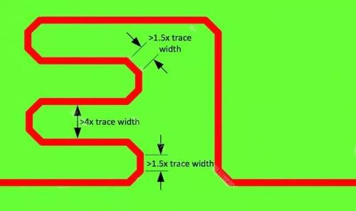
With exception of RF signals and other signals with special requirements, it is desirable to have tracks on our PCB at a 45° angle. It should be noted that when tracks at a 45° angle are of same length, length of track at corner must be at least 1.5 times width of line, and distance between lines of equal length must be at least 4 times width of line. line width. Since a high-speed signal line is always transmitted along path with lowest impedance, if distance around lines of same length is too close, high-speed signal will be shortened due to parasitic capacitance between lines, and equal length will be inaccurate. The winding rules of modern EDA software can easily set corresponding winding rules.
Arc route arc
Unless it is a technical specification that explicitly requires arc tracing or high-frequency microwave transmission lines, Mr. Wu personally believes that there is no need to use arc lines, because arrangement of high-speed and high-density pcb requires a large number of arc lines, which will later be restored. The lines are very troublesome, and a large number of curved lines also take up space.
Of course, it is still preferable to use a curved line or even a 45° outside bevel line for RF microwave transmission line.
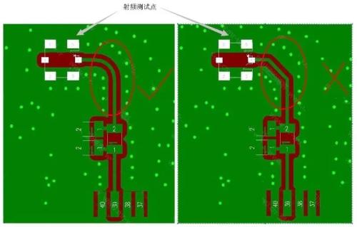
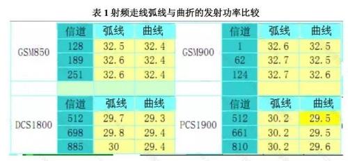
The figure below is result of comparing actual transmission power measurement of RF transmission line arc and 45° curve. It can be proven that arc of high-frequency signal is indeed due to 45°. ° trace angle.
Route at any angle
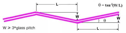
With development of 4G/5G wireless communication technology and constant upgrading of electronic products, current transmission rate of PCB interface has reached 10Gbps or 25Gbps, and signal transmission rate is still rising towards high speed. With development of high-speed and high-frequency signal transmission, higher demands are placed on PCB impedance control and signal integrity. For digital signals transmitted on printed circuit boards, many dielectric materials used in electronics industry, including FR4, are considered to be uniform at low speed and low frequency transmission. However, when electronic signal rate on system bus reaches Gbps level, this assumption of uniformity ceases to be true, at which time gap between fiberglass strands woven into epoxy resin substrate causes relative dielectric constant of dielectric layer to localize. The change will not be insignificant, and local perturbation of permittivity will make time delay and impedance of line coupled to space, which will affect transmission of high-speed signals. The test data based on FR4 test substrate shows that due to relative position difference between microstrip line and glass fiber bundle, measured effective dielectric constant of transmission line fluctuates greatly, and difference between maximum and minimum values can reach △εr=0.4. Although these spatial perturbations appear to be small, they can seriously affect differential transmission links at data rates of 5-10 Gb/s.
In some high-speed design projects, in order to cope with effect of fiberglass effect on high-speed signals, we can use zigzag wiring technology to slow down effect of fiberglass effect.
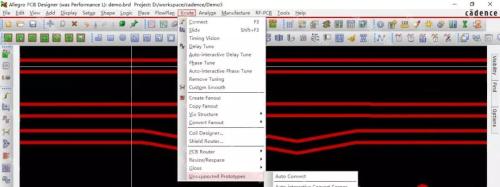
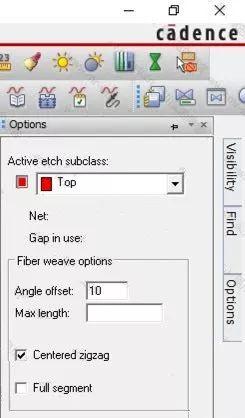
Cadence Allegro PCB Editor 16.6-2015 and later supports zigzag layout.
From Cadence Allegro PCB Editor 16.6-2015 menu, select Route -> Unsupported Prototype -> Fiber Weave Effect to open zigzag routing feature.
Just like twenty years ago, our PCB layout didn't have to pay attention to whether or not to follow arc line, and we didn't have to worry about effects of PCB's fiberglass plate on high-speed signal.
Therefore, there are no fixed PCB layout rules. With improvement of PCB manufacturing process and increase in data transfer rates, it is possible that current correct rules will become inapplicable in future. Therefore, most qualified traction wire bacteria must keep pace with times and master development of industrial technology, so as not to be eliminated by large waves.
Related
- Should PCB trace angle be 90°? — Jumping guide to PCB layout pit
- Can a PCB trace angle be 90 degrees?
- Diagram of relationship between PCB layout and EMC
- Do you know layout requirements of some special devices in PCB design?
- PCB design guidelines: safety regulations, layout and wiring, EMC, thermal design, process engineering.
- Pay attention to PCB vias
- How to make anti-interference PCB design?
- Why can't crystal oscillator be placed on edge of the PCB?
- Surprisingly, this is most prone to PCB failure?
- Case analysis! Why can't crystal oscillator be placed on edge of PCB?
Hot Posts
 How to distinguish induction from leakage, we will teach you three tricks! Ordinary people can also learn super practical
- What is drowning in gold? Why Shen Jin?
- This is a metaphor for EMI/EMS/EMC that can be understood at a glance.
- How many types of pads have you seen in PCB design?
- Summary of Common PCB Repair Techniques
- What is three anti-paint? How to use it correctly?
- Knowing these rules, you will not get confused looking at circuit diagram.
- How to make anti-interference PCB design?
- Can diodes do this?