Location:Home Page > Archive Archive
Does PCB use copper mesh or solid copper, are you using it correctly?
2023-04-03【Archive】
1 What is a copper fill
The so-called copper pouring consists of using unallocated space on a flexible printed circuit board as a reference plane and then filling it with solid copper. These areas of copper are also referred to as poured copper.
Copper pouring value: lower ground wire impedance, improve anti-jamming; In addition, in order to prevent distortion of PCB during soldering, most PCB manufacturers also require PCB designers to fill open area of the PCB with copper or mesh ground wires. right, gain does not compensate for loss, is copper plating "advantage outweighs disadvantages" or "disadvantages outweigh advantages"?
Everyone knows that in case of a high frequency, distributed capacitance of wiring on printed circuit board will work. At a wavelength greater than 1/20 of wavelength corresponding to frequency of noise, an antenna effect will occur, and noise will pass through wiring to external radiation, if in printed board has a badly grounded copper pot, copper pot will become a tool for noise propagation. wiring less than λ/20 to be "well grounded" with ground plane of multilayer board. With proper handling of copper sheath, copper sheath can not only increase current, but also play dual role of shielding interference.
2 Two Copper Pour Shapes
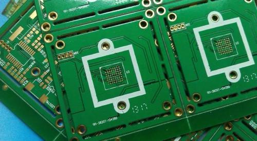
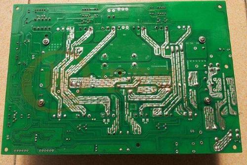
Typically, there are two main methods for pouring copper, namely pouring copper over a large area and pouring mesh. It is often asked whether it is better to pour copper over a large area. area The grid is covered with copper, but it is not good to generalize. Why? A large area of copper plating has dual function of increasing current and shielding, but if a large area of copper plating is subjected to wave soldering, board may warp or even bubble. Therefore, for large area copper cladding, several slots are usually opened to reduce copper foil bubbling. As shown below
Pure copper mesh mainly shields, and current increase effect is reduced. In terms of heat dissipation, mesh is beneficial (reduces heating surface of copper) and plays a role in electromagnetic field. shielding. Especially for circuits such as touch, as shown in figure below.
It should be noted that grid consists of tracks arranged in a checkerboard pattern. We know that for a circuit, trace width has corresponding "electrical length" for PCB operating frequency (actually divide size by digital frequency corresponding to operating frequency, see relevant books for details), when operating frequency is not very high, perhaps influence of grid line is not very obvious, once electrical length matches operating frequency, this is very bad, you will find that circuit does not work properly at all, and signal is radiated all over place, which interferes with operation of system.
The suggestion is to choose according to working conditions of designed PCB, and not cling to one thing. Therefore, for solid copper laying, multi-purpose networks with high noise immunity requirements for high-frequency circuits and high-current circuits for low-frequency circuits are usually used.
Related
- Does PCB use copper mesh or solid copper, are you using it correctly?
- What is three anti-paint? How to use it correctly?
- Is printed circuit board covered with copper very “up to mark”? One article to help you get practical guidelines and norms
- Why can't copper and aluminum wires be twisted together when wiring?
- Can you answer these questions about using capacitors?
- Daniel's Summary: The details and experience of 30 PCB layouts are wonderful.
- Did you pay attention to details of using relay?
- How many types of pads have you seen in PCB design?
- Do you know layout requirements of some special devices in PCB design?
- A list of most common PCB design mistakes, see how many mistakes have you made?
Hot Posts
 How to distinguish induction from leakage, we will teach you three tricks! Ordinary people can also learn super practical
- What is drowning in gold? Why Shen Jin?
- This is a metaphor for EMI/EMS/EMC that can be understood at a glance.
- How many types of pads have you seen in PCB design?
- Summary of Common PCB Repair Techniques
- What is three anti-paint? How to use it correctly?
- Knowing these rules, you will not get confused looking at circuit diagram.
- How to make anti-interference PCB design?
- Can diodes do this?