Location:Home Page > Archive Archive
Is printed circuit board covered with copper very “up to mark”? One article to help you get practical guidelines and norms
2023-04-03【Archive】
1. When covering platform with copper, it must be completely covered, and mold and platform cannot form an acute angle.
2. Try to use copper wires instead of thick ones. When thick lines are used, vias are usually fancy routing vias that increase aperture and surface of via.

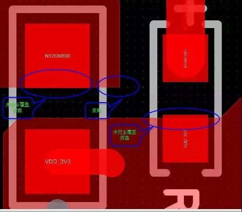
3. Consider using a copper fill instead of copper fill + trace pattern, which often produces small sharp corners and right angles. Use copper fill instead of tracing.
4. The form border must be at a grid point, no grid is allowed. (Sony specification)
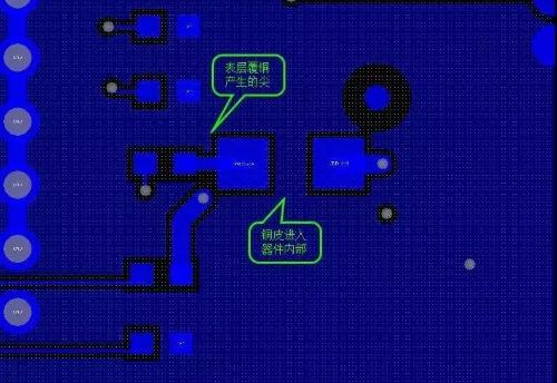
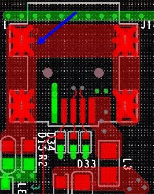
5. The corners of form must be same size. As shown in image below, both sides of a corner are 4 grid points, so all small corners should be same size. The shape cannot cross platform and penetrate inside device, in particular, surface layer is covered with copper over a large area.
6. Strictly speaking, form and form, form and line, must be placed at same distance from each other. If distance between figure and line is set to 0.3 mm, then distance between all figures should be same. There can't be situations like 0.4mm. or 0.25 mm., but in order to keep copper on grid, this is distance of grid, subject to a distance of 0.3 mm.
7. Plug body ground, GND at other end of inductance connected to body ground, and other end of the resistor are copper plated.
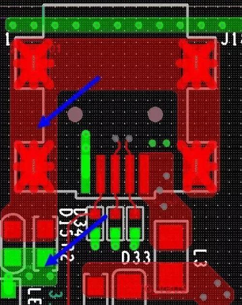
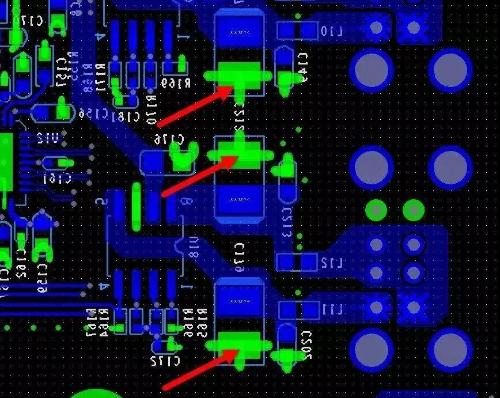
8. The copper plug sheath connection method uses 8 corner method, not full connection method.
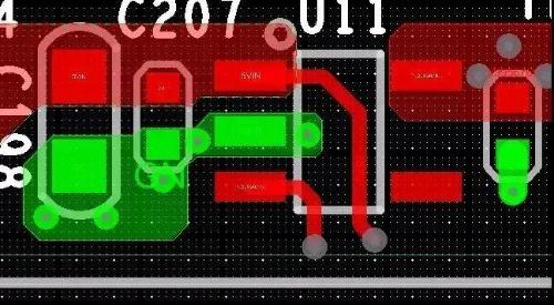
9. The GND terminal of capacitor directly enters ground of inner layer through through hole, do not connect through copper shell, latter is not conducive to welding, and copper shell in a small area is useless.
10. The connection of power supply, especially output of power supply from power supply chip, is connected by pouring copper.
11, PCB, even if there are many empty areas, if distance between signal lines is large enough, there is no need to cover surface with copper. Partial copper plating on surface will result in an uneven balance of copper foil on PCB. And if copper fill is too close to trace, trace impedance will be affected by copper jacket.
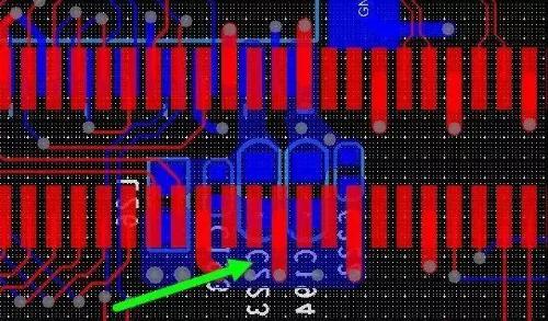
12. Due to limited space, GND cannot enter inner ground layer through adjacent through hole. At this time, it can be connected to inner ground layer through local copper potting and then through through hole.
Related
- Is printed circuit board covered with copper very “up to mark”? One article to help you get practical guidelines and norms
- One article eats up all rectifier and filter circuits
- You must learn drawing techniques and skills of 18 special circuit board routes.
- How many of these free and easy to use circuit design programs have you used?
- Understand Current Detection Circuit in One Article
- What is difference between surge device, lightning arrester, leakage protection, circuit breaker and circuit breaker? Come and get knowledge
- Hardware Circuit Design Specification: A Very Good Reference to Hardware Design
- Three circuit diagrams to teach you how to understand how a buck RC works
- An article to understand "advantages" and "cons" of solid capacitors
- Diode switching circuit and troubleshooting, one complete wizard
Hot Posts
 How to distinguish induction from leakage, we will teach you three tricks! Ordinary people can also learn super practical
- What is drowning in gold? Why Shen Jin?
- This is a metaphor for EMI/EMS/EMC that can be understood at a glance.
- How many types of pads have you seen in PCB design?
- Summary of Common PCB Repair Techniques
- What is three anti-paint? How to use it correctly?
- Knowing these rules, you will not get confused looking at circuit diagram.
- How to make anti-interference PCB design?
- Can diodes do this?