Location:Home Page > Archive Archive
Common USB Interface Circuit Design Problems and Solutions
2023-04-10【Archive】
USB is a fast, two-way, synchronous, low-cost, easy-to-use, hot-swappable serial interface.
Because of advantages of fast data transfer, user-friendly interface, and hot plug support, USB devices are widely used. At present, most of products on market use USB2.0 as interface, but many newcomers to equipment encounter many problems in USB applications, and there are often various problems with USB interface after PCB is assembled.
For example, if connection is unstable or cannot communicate, check circuit and soldering, and there is no problem. It may be necessary to suspect at this time that circuit board design is unreasonable. Rendering a PCB that meets USB 2.0 data transfer requirements plays an extremely important role in product performance and reliability.
The USB protocol specifies that two differential signal lines (D+, D-) carry digital signals. For a USB device to work stably, differential signal line must be laid in strict accordance with differential signal rules. According to author's many years of experience in developing and debugging USB related products, following points can be summarized:
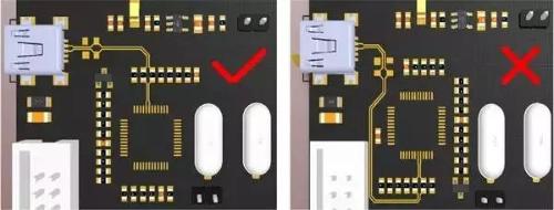
2. Give priority to drawing differential lines. Try not to exceed two pairs of vias on a pair of differential lines (vias will increase parasitic inductance of line, which will affect signal integrity of line). and you need to arrange them symmetrically (√ - a reasonable way, × - unreasonable);

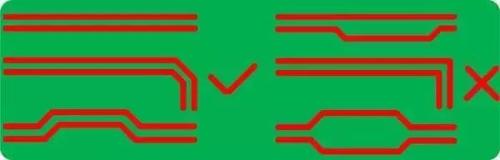
3. Symmetrical parallel routing that provides a tight connection between two wires and avoids 90° routing. The best laying methods are arc or 45° (√ is a reasonable way, × is an unreasonable way);< /strong>
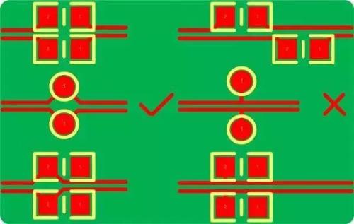
4. Placement of differential series resistors, test points, and pull-up resistors (√ is smart way, × is unreasonable way);
5. Due to factors such as pin distribution, vias, and routing space, differential line lengths do not easily match. If line lengths do not match, timing is shifted and common mode noise appears. ., reducing signal quality. Therefore, compensation for mismatch of differential pair must be made accordingly so that lengths of lines match. The length difference is usually controlled within 5 mils. Compensation principle - where does length difference occur and where to compensate;< /p>
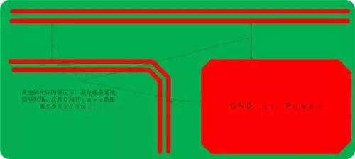
6. To reduce crosstalk, if space permits, distance between other signal networks and ground should be at least 20 mils from differential line (20 mils is a rule of thumb), and distance between ground and differential line is too close. Affects line impedance;
7. USB output current is 500 mA. Pay attention to width of VBUS and GND lines. If 1 ounce copper foil is used, a line width of more than 20 mils can meet current requirements. Of course, wider line width, fuller power supply, better.
The signal line width and line spacing of differential line of conventional USB devices must match signal line width and line spacing of entire board. However, when operating speed of USB device is 480Mbps, it is not enough just to achieve above points. We also need to control differential signal impedance. It is very important to control differential signal line impedance. for high speed digital signal integrity.
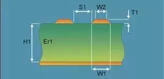
Because differential impedance affects eye diagram, signal bandwidth, signal jitter, and interference voltage on differential signal signal line. Line differential impedance is typically adjusted to 90 (±10%) ohms (see chip manual for specific values). The differential line impedance is inversely proportional to line width W1, W2 and T1 and inversely proportional to permittivity. Er1, and proportional to line spacing S1., which is proportional to distance H1 to reference layer. The following figure shows a cross section of a differential line.
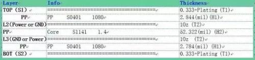
The figure below shows reference stack of a four-layer board, in which two middle layers are reference layers, reference layer is usually GND or Power, and reference layer corresponding to differential line must be full and cannot be separated, otherwise differential line will be damaged Impedance discontinuity. If a four-layer board is constructed as shown in Fig. 2, width of differential line and line spacing of 5.5 mils can meet differential impedance of 90 ohms.
However, 4.5 mil line width and 5.5 mil line spacing are just our theoretical values. required impedance value, combined with the actual production situation and board adjustment.
The connection rules described above are based on USB 2.0 devices. In USB connection process, use shortest differential lines, tight connection, same length and constant impedance, and pay attention to current carrying capacity of USB power supply. Familiarize yourself with principles described above USB The device operates mostly normally.
Related
- Common USB Interface Circuit Design Problems and Solutions
- Frequently Asked Questions for USB Interface Circuit Design
- Three common grounding methods in circuit design
- Senior EMC Engineer Resume: EMC Troubleshooting Process and Common Problems
- How many of these free and easy to use circuit design programs have you used?
- Industrial Computer Circuit Design
- Hardware Collection: 50 Common Circuit Diagrams
- Hardware Circuit Design Specification: A Very Good Reference to Hardware Design
- How to design a triode amplifier circuit
- 50 Common Hardware Design Patterns
Hot Posts
 How to distinguish induction from leakage, we will teach you three tricks! Ordinary people can also learn super practical
- What is drowning in gold? Why Shen Jin?
- This is a metaphor for EMI/EMS/EMC that can be understood at a glance.
- How many types of pads have you seen in PCB design?
- Summary of Common PCB Repair Techniques
- What is three anti-paint? How to use it correctly?
- Knowing these rules, you will not get confused looking at circuit diagram.
- How to make anti-interference PCB design?
- Can diodes do this?