Location:Home Page > Archive Archive
3 Common Misconceptions When Designing Differential Signals on PCBs
2023-05-03【Archive】
In high-speed printed circuit boards, a differential signal (DIFFERENTIAL SIGNAL) is increasingly used, and most important signal in a circuit often has a differential structure.
Why? Compared with ordinary single-ended signal tracks, differential signals have advantages of strong anti-interference ability, effective EMI suppression, and accurate time positioning.
01
Wiring Requirements
On a printed circuit board, differential tracks should be two lines of same length, same width, located in close proximity to each other and at same level.
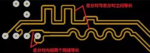
▶ Same length:
Equal length means that two lines should be as long as possible so that two differential signals always maintain opposite polarity. reduce common-mode components.
▶ Monospace, monospace:
Equal width means that trace width of two signals must be same, and equidistant means that distance between two lines must remain same and parallel.
▶ Minimum impedance change:
One of most important things when designing a PCB with differential signals is determining target impedance of application and then planning differential pairs accordingly. Also make sure that impedance changes are as small as possible. The differential line impedance depends on factors such as track width, track connection, copper thickness, PCB material, and layout. Consider each of these when trying to avoid anything that changes impedance of a differential pair.
02
Common misconceptions
Misconception 1. Think that differential signals don't need to be grounded as a return path, or that differential traces provide each other with a return path.
The reason for this misunderstanding is that you are confused by superficial phenomena, or you do not understand mechanism of high-speed signal transmission deeply enough. Differential circuits are insensitive to similar ground signals and other noise signals that may be present on power and ground planes.
Partial ground plane reverse flow suppression does not mean that differential circuit does not use reference plane as signal return path. In fact, when analyzing reverse flow of a signal, mechanism of differential routing and conventional single-ended routing is serial, that is, high-frequency signal always flows back along loop with least inductance. whatever type of connection is strong, will become main backflow.
In PCB circuitry, coupling between differential traces is generally small, often only 10-20% of degree of coupling, and coupling to ground is greater, so main return path of differential traces still exists. at ground level.
If there is a break in ground plane, connection between differential traces will provide a primary return path in area without a reference plane, although a break in reference plane does not affect differential traces. this is serious after all, but it will still reduce quality of differential signal and increase EMI, which should be avoided as much as possible.
In addition, some designers believe that reference plane under differential trace can be removed to suppress some of common signal in differential transmission, but this approach is theoretically impractical. How to control impedance? The absence of a reverse impedance path for common-mode signals will necessarily cause electromagnetic radiation that does more harm than good.
Myth #2: Thinking equal spacing is more important than string length matching.
In actual PCB layout, it is often impossible to meet differential design requirements at same time. Due to factors such as pin distribution, vias, and wiring space, goal of line length matching must be achieved by proper winding, but as a result, some areas of differential pair cannot be parallel.
The most important rule when designing differential PCB routing is line length. Other rules can be applied flexibly according to project requirements and practical applications.
Misunderstanding 3. Think differential traces should be close together.
Shorting differential tracks is nothing more than strengthening their coupling, which can not only improve noise immunity, but also make full use of opposite polarity of magnetic field to compensate for electromagnetic interference to outside world.
While this approach is very beneficial in most cases, it is not absolute. If we can ensure that they are completely shielded from outside interference, then we won't need to go through each other's strong coupling. The goal of anti-interference and EMI suppression has been achieved.
How can we ensure good isolation and shielding of differential traces? This is one of most basic ways to increase distance between traces of other signals. The energy of electromagnetic field decreases with square of distance. Generally, when distance between lines exceeds 4 times line width, interference between them is extremely weak, basically can be ignored.
In addition, isolation through ground layer can also play a good shielding role. This structure is often used in design of high frequency (above 10G) IC circuit boards. It is called CPW structure, which can provide strong differential impedance. control.
Related
- 3 Common Misconceptions When Designing Differential Signals on PCBs
- Ten Misunderstandings Often Faced by Hardware Engineers When Designing Circuit Stability
- When designing a power supply, how to consider choice of topology?
- What skills should I pay attention to when designing a triode amplifier circuit? (Easy to understand)
- 10 Misconceptions About Chain Reliability, Have You Been Hired?
- Popularizing common sense inductors
- Common Mistakes of Electronics Engineers
- 50 Common Hardware Design Patterns
- Summary of Common PCB Repair Techniques
- Hardware Collection: 50 Common Circuit Diagrams
Hot Posts
 How to distinguish induction from leakage, we will teach you three tricks! Ordinary people can also learn super practical
- What is drowning in gold? Why Shen Jin?
- This is a metaphor for EMI/EMS/EMC that can be understood at a glance.
- How many types of pads have you seen in PCB design?
- Summary of Common PCB Repair Techniques
- What is three anti-paint? How to use it correctly?
- Knowing these rules, you will not get confused looking at circuit diagram.
- How to make anti-interference PCB design?
- Can diodes do this?