Location:Home Page > Archive Archive
When designing a power supply, how to consider choice of topology?
2023-04-25【Archive】
01 Summary
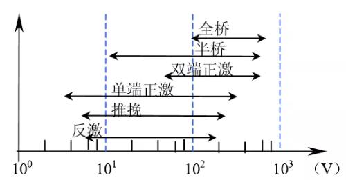
Input voltage and output/input ratio are important considerations when choosing a topology. On fig. 1 shows relative applicable voltage ranges for commonly used isolated topologies. The choice of topology is also related to output power, number of output voltage circuits, and output voltage adjustment range. In general, multiple topologies can be applied for a given case. It cannot be said that a certain topology is absolutely suitable for a certain application, because design of product also includes experience of designer with a certain topology, whether it is easy to obtain components, etc. Related factors are, such as cost requirements, technical staff requirements, debugging equipment and personnel quality, manufacturing process equipment, batch size, military or civilian products, etc. Therefore, in order to select best topology, you must be familiar with strengths and weaknesses of each topology and scope of topology. If you choose a topology at random, you may declare new power supply design a failure from start.
02 Input and Output
If output and input share same ground, you can use a non-isolated buck and boost converter with a common ground. These circuits are simple in structure and contain few components. If input voltage is high, it is usually necessary to isolate output from input for safety reasons.
Before choosing a topology, you must first know if output voltage is higher or lower than input voltage within input voltage range? For example, a buck converter can only be used when output voltage is lower than input, so output voltage must always be lower than input. If you require 24V input and 15V output, you can use Buck topology; but if 24V input changes from 8V to 80V, you cannot use a buck converter because a buck converter cannot convert 8V to 15V. If output voltage is always higher than input voltage, Boost topology must be used.
If ratio of output voltage to input voltage is too high (or too low), there is a limitation. For example, if input voltage is 400V and output must be 48V, or a buck converter is used, voltage ratio is too large, although output voltage is always lower than input voltage. But such a large voltage ratio, although not exceeding minimum duty cycle range control chips, limits switching frequency. In addition, peak current of power device is large, and selection of power device is difficult. If an isolated topology is used, appropriate duty cycle can be adjusted using turns ratio. To achieve best value for money.
03 Practical limits for switching frequency and duty cycle
1. Switching frequency
When designing a converter, first step is to select switching frequency. The main purpose of increasing frequency is to reduce size and weight of power supply. The magnetic components account for bulk and weight of power supply. In today's switching power supplies, magnetic components account for volume (20% to 30%) of switching power supply, weight (30% to 40%), and loss of 20% to 30%. According to the law of electromagnetic induction:

In formula, U is voltage supplied by transformer; N-turns of coil; A is cross-sectional area of the core; ΔB-change in magnetic flux density; f is operating frequency of transformer.
At lower frequencies, ΔB is limited by saturation of magnetic material. It can be seen from above formula that at a constant U, to reduce volume of magnetic circuit, product of number of turns and cross-sectional area of the magnetic circuit is inversely proportional to frequency, and increasing frequency is main measure to reduce volume of power supply. This has been a major research topic for countless scientists and technicians since advent of switching power supplies.
But is it possible to increase frequency of a switching power supply indefinitely? No. There are two main limiting factors: The first is loss of magnetic material. Ferrite is commonly used at high frequencies and its loss per unit volume is expressed as:
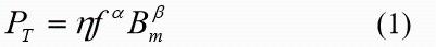
In formula, η is coefficient of various materials, f is working frequency, Bm is working amplitude of magnetic induction. α and β - indicators of degree of loss of frequency and magnetic induction, exceeding 1, respectively. Usually α=1.2~1.7, β=2~2.7. The frequency increases and loss increases. In order to reduce loss, at high frequency, magnetic induction Bm is reduced so that loss is not too large, which defeats purpose of volume reduction. Otherwise, losses will be too great, and efficiency will decrease. In addition, larger processing power of magnetic core, larger volume and worse heat dissipation conditions, and powerful magnetic core also limits switching frequency.
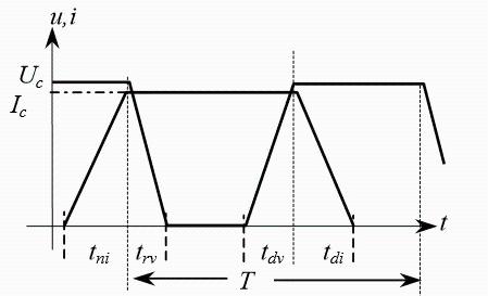
Secondly, switching losses of power devices are limited. Take as an example a buck converter illustrating switching losses. Rice. 2 is a typical current and voltage waveform diagram across a power tube of a buck-DC converter. It can be seen that when transistor is turned on, collector voltage begins to drop when collector current increases to a maximum value. When turned off, collector voltage first rises to a maximum value, and collector current begins to fall. It is assumed that rise and fall of voltage and current are linear. The switching loss can be obtained as
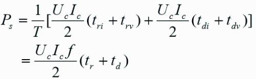
In formula tr=tri trv is sum of current rise time and voltage fall time when turned on; td=tdi tdv is sum of voltage rise time and current fall time when it is turned on. switched off. Usually tr td

If current is discontinuous, only turn-off losses, switching losses:

It can be seen that switching losses are proportional to switching frequency and switching time. The intermittent current accounts for less than half of continuous switching loss, but it should be noted that at same output power, power lamp current is at least twice that of direct current. In addition to increasing current rating and cost of device. increases, conduction voltage drop losses also increase. The magnetic core of filter inductor works as a direct transformer, and high-frequency loss of magnetic core and coil will also increase significantly. Although switching losses can be reduced with soft switching technology, please note that soft switching always uses LC resonance, resonant current (or voltage) is very large, and resonant current passes through transistor, inductor L and capacitor C, and these components also with losses. Sometimes efficiency increases by only 1-2%, but circuit becomes more complicated, number of components increases, cost increases, and sometimes gain exceeds gain.
Currently, power of MOSFET switches is below 5kW, and operating frequency is usually below 200kHz. BYuT up to 50 kHz. More than 3 kW uses highest 30 kHz IGBT. The highest combined MOSFET and IGBT lamp (BJT) does not exceed 100 kHz. The conversion power is tens of watts, and, of course, operating frequency can be increased.
In addition, greater conversion power, greater current and voltage. If current rise and fall rate of high-power lamp is same as that of low-power lamp, high-power lamp requires a longer switching time. What's more, chip area of high-power devices is large, and switching time is also extended to avoid current concentration and reduce current rise and fall rate during switching. It can be seen that greater conversion power, lower permissible switching frequency.
If you have heard that operating frequency of its switching power supply can reach several MHz, you must ask how much conversion power does it have?
2. Working cycle
The conversion ratio (ratio of output voltage to input voltage) of switching converters is limited if it is too high or too low. Firstly, duty cycle of converter (the ratio of switch conduction time to switching period) is limited by maximum and minimum values of control chip. In some topologies, duty cycle cannot exceed 0.5. In short, general purpose PWM control ICs generally do not guarantee that duty cycle can be greater than 0.85; some ICs do not guarantee that duty cycle will be below 0.05 in order to quickly drive gate of a MOSFET with little loss at an acceptable operating frequency.
For example, if switching frequency is 250 kHz and period is 4 µs, if duty cycle is 0.1, turn-on time of MOSFET isthe history is only 0.4 µs, and if turn-on time of MOSFET is 0.1 µs, turn-off time is also 0.1 µs, which is almost same as part of conduction time is “eaten up” by transition time, and losses increase. This is one of reasons why higher conversion power, lower operating frequency.
Regardless of control IC, high current gate drive, etc., as long as you don't design a duty cycle beyond minimum 0.1 and maximum 0.8 (0.45 for converters limited to 0.5), you will not will worry about it.
If topology used has a transformer, factor can adjust duty cycle. But transformation ratio is also limited. If turn ratio is too large or too small, difference in size between primary and secondary wires is too great and it will be difficult to wind coil. Typically, maximum ratio of primary to secondary windings is 10:1 and minimum is 1:10. If you need to get a high voltage from a very low voltage, consider using a two-stage converter or a secondary voltage doubling circuit to boost voltage.
04 How many outlets?
The next question after work cycle is how much to output. For example, Buck is not suitable if it is not 1 output. In some cases an additional regulator can be added to produce a different voltage, a practical example would be a buck converter to create a 5V output and a linear regulator (or other switch) to create a 3.3V output from a 5V input. However, corresponding transients , noise and loss must meet requirements.
Worst case scenario, design multiple independent transducers instead of complex magnetic components with multiple coils. Before you start designing, you should consider that if you use a converter with multiple outputs, you can save a few dollars on a control IC, but you can spend tens of dollars on a complex magnetic component with multiple coils. Before designing, you must first weigh magnetic components, circuit components, and additional costs, and not just talk about it.
05 Quarantine
Before designing, it is necessary to know in advance whether it is necessary to isolate secondary and primary. If input is powered by mains or high voltage, like a commodity, there are safety regulations (and EMI issues) that require isolation. A typical example is that input and output have a withstand voltage requirement of 500 VAC. Once you know security requirements, some topologies like Buck without isolation, Boost, etc. will be excluded.
EMI 06
Think about EMI at start, do not wait until project is completed to consider EMI. Some topologies can be very successful in preventing EMI problems. If it is a non-isolated system, since there is no third wire such as a battery in system, there will be no common mode noise, making filtering easier.
In addition, some topologies generate more noise than others. The difference is that some topologies are disconnected from input for part of each cycle, causing input current to break. If input current is continuous, there will be no rising and falling edges, current will not be zero and it will be easy to filter.
The buck converter is an example of intermittent input current because when switch is open, input current is zero. The inductance of boost converter is always connected to input circuit, but whether input current is continuous depends on whether boost converter is operating intermittently or continuously.
The author recommends against using discontinuous input current topologies in high-power power supplies, as such topologies usually require expensive magnetic components.
07 BJT, MOSFET or IGBT?
The choice of topology depends on available power devices. Power devices currently available include bipolar (BJT) power tubes, MOSFETs, and IGBTs. The rated voltage of bipolar tube can exceed 1.5kV, commonly used below 1kV, and current ranges from a few mA to hundreds of A; MOSFET is below 1KV, generally used below 500V, and current is from A to hundreds of A. ; Up to several kV, current from tens of A to several kA.
Different devices have different control requirements: bipolar transistors are current driven, high power high voltage transistors have low current gain and are often used in single switch topologies. In low to medium power range, 90% choose MOSFETs, except for special reasons.
One of reasons is cost. Bipolar lamps are still cheaper than MOSFETs if volume of product is large. But use of bipolar power tubes means that switching frequency is lower than MOSFETs, so volume of magnetic components is relatively large. Is it still worth it? You will have to take a close look at research costs.
If input voltage is high (380V) or push-pull topology plus transient voltage requires more than twice voltage, you may find it difficult to choose a power lamp. If you use a bipolar lamp, you can buy a 1500V bipolar tube, and maximum MOSFET voltage you can currently buy is 1000V, and on-resistance is greater than BJT. Of course, you can consider using an IGBT. Unfortunately, although an IGBT drive is similar to a MOSFET, its switching speed is similar to that of a MOSFET.and polar lamp, which has serious problems with tail.
It can be seen that below low voltage (500V) this is basically MOSFET world, and low power switching frequency (hundreds of watts) is hundreds of kHz. The rated voltage of IGBT is usually over 500V and current is over tens of amps. It is mainly used for speed control and mainly replaces high voltage bipolar darlington tube. The operating frequency can reach 30 kHz, usually about 20 kHz. Due to large conduction voltage drop, it is not used below 100 V.
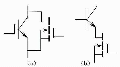
To improve switching speed of IGBT or BJT, MOSFET and BJT or IGBT can also be combined into a composite tube. Bipolar transistor U(BR) CBO/70A in fig. 3(b) is connected in series with a 50V/60A MOSFET that is used in input of a 380V (510V) three-phase rectification inductance filter of a 3kW two-pole feedforward. power supply. When it is turned on, power MOSFET is first driven. At this time, bipolar transistor operates in a configuration with a common base and emitter input current, or since MOSFET is turned on and drain voltage drops, emitter junction of forward-biased bipolar transistor generates current base, resulting in a collector current. Positive feedback is formed through a proportional control circuit, which makes BJT saturated and on. When it is off, MOSFET is first turned off and emitter junction is reverse-biased so that BJT turns off quickly. The overall basic frequency response is β times that of common emitter. Improved shutdown speed. The on-resistance of a low-voltage MOSFET is only on order of mΩ, and conduction losses are very small. The actual operating frequency of circuit is 50 kHz.
Parallel connection of MOSFET and IGBT also uses switching characteristics of MOSFET. To achieve this goal, control of MOSFET and IGBT should be designed in such a way that when turned on, PWM signal can make MOSFET turn on at same time or first, and then turn on IGBT. IGBT conductance at zero voltage. When turning off, IGBT turns off first, and IGBT turns off at zero voltage, after a certain delay, MOSFET turns off. MOSFET incurs switching losses; during conduction period, conduction voltage drop of high-voltage MOSFET is larger than that of IGBT, and most of current flows through IGBT, allowing IGBT to bear conduction loss. A practical example of this combination operates at 50 kHz with a 3 kW half-bridge topology.
08 Continuous or intermittent
Inductance (including flyback transformers) and current (ampere-turns) continuous or intermittent: In a discontinuous mode converter, inductor current is zero at some point in cycle. Continuous current (ampere-turn) means that there must be enough inductance to maintain minimum load current ILmin (including dummy load), and inductance must be current at any point in cycle. This
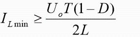
Among them, T-switching period, D=Ton/T-duty cycle, Ton-transistor conduction time. We assume that forward voltage drop of rectifier is small compared to output voltage. If minimum load current is zero, you should enter hiccup mode.
In actual design of power supply, common power supply has no-load requirements, and inductance cannot be too large. It should be intermittent at low loads. In this case, a dummy load is sometimes set, and when load current exceeds dummy load. Otherwise, it may cause problems with stability of feedback control, and feedback compensation network must be carefully designed.
Synchronous patching is an exception. Converters using synchronous rectification always operate in continuous mode and do not require a minimum inductance.
09 Synchronous Fix
Today, in many low-output applications, converter efficiency is (almost) more important than cost. More expensive but highly efficient converters are actually cheaper from a user's point of view. If computer has low power efficiency, actual computing time is often very short and latency is very long, which will cost more on electricity bill.
If efficiency is important, consider synchronous rectification. That is, a MOSFET is used in output rectification. Many driver IC chips are available today that can drive both FETs and synchronous rectifiers very well.
Another reason to use synchronous rectification is that it converts a converter operating in intermittent current mode to DC mode. This is because current can flow in both directions even when there is no load (because MOSFETs can conduct current in both directions). The use of synchronous rectification saves you worry of mode change (which can make converter unstable) and ensures continuous minimum inductance requirements.
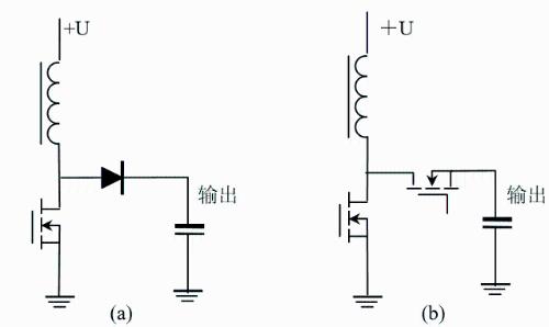
The question of synchronous rectification is worth mentioning here. The main switch turns off before synchronous rectification turns on and vice versa. If this is neglected, breakdown will occur when input (or output) voltage is shorted directly to ground, resulting in large losses and possible failure. During turn off of both MOSFETs, inductor current is still flowing. Normally no current should flow through diode in MOSFET package due to long recovery time of this diode. For example, body diode is supposed to pass current when MOSFET is turned off. When body diode recovers, it acts as a reverse-recovery short circuit, so as soon as input (or output) is connected to ground, breakdown occurs, which can lead to output converter failure, as shown in Figure 4(b).
To solve this problem, a Schottky diode can be connected in parallel with MOSFET's internal diode to allow current to flow when FET is off. (Since forward voltage drop of Schottky diode is lower than that of body diode, almost all of current flows through Schottky, and reverse recovery time of body diode is related to forward current before turning off, so it can be neglected at this time)
10 Voltage mode and current mode control
When designing a switching power supply, it should be considered in advance whether to use voltage or current control mode, which is a control problem. Almost every topology can use any of them. Current mode control can limit current cycle by cycle, and overcurrent protection becomes easy to implement. At same time, magnetic bias of output transformer can be overcome for push-pull or bridge converters. But if current is large, then a sense resistor (which consumes a lot of power) or a transformer (which costs a lot of money) is required to determine current, which may affect your choice. However, detection of overcurrent protection runs smoothly. However, if you use a current control type for a half-bridge converter, this can lead to a voltage imbalance in capacitor dividing voltage. So for high power output, you should consider which one is better.
11 Conclusion
It's best to know system your power supply will run on before designing power supply. Learn more about power requirements and limitations of this system. A complete understanding of system can significantly reduce costs and design time.
In real work, you can list specifications required by converter and consider each element. You'll find that these specifications limit you to one or two topologies to choose from, and it's easy to choose a topology based on cost and size. Usually, topology can be chosen based on various considerations above:
① Boost or Step Down: Is output always higher or lower than input? If not, you cannot use Buck or Buck/Boost.
② Duty cycle: Is ratio of output voltage to input voltage greater than 5? If yes, then you probably need a transformer. Calculate duty cycle to make sure it is neither too long nor too short.
③ How many sets of output voltage do you need? If it is greater than 1, unless a downstream regulator is added, a transformer is usually required. If there are too many output groups, it is recommended to use multiple converters.
④ Is insulation required? What voltage? For isolation, a transformer is needed.
⑤ What are EMI requirements? If requirements are stringent, then it is recommended not to use intermittent input current topology of Buck type, but to select current continuous mode of operation.
⑥ Is cost extremely important? BJT can be selected for low power and high voltage. If input voltage is higher than 500V, IGBT can be considered. Use MOSFETs instead.
⑦ Do you need to unload power supply? If necessary, select intermittent mode, unless question 8 is used. You can also add a dummy load.
⑧ Can synchronous rectification be used? This makes converter current continuous regardless of load.
⑨ Is the output current large? If so, you should use voltage type instead of current type.
Related
- When designing a power supply, how to consider choice of topology?
- How to intelligently prevent positive and negative poles of a power supply from being reversed?
- Four ways to reduce the output "ripple and noise" of a switching power supply
- How does internal resistance affect a power supply?
- What is power supply ripple, how to measure their magnitude and how to suppress?
- Analysis of damping RC circuit of a switching power supply "haberdashery"
- Detailed analysis of the "various protection schemes" of a switching power supply
- Analysis of various losses inside a switching power supply from 4 aspects
- Finally, it becomes clear that process of obtaining switching losses of a MOSFET in a switching power supply
- What skills should I pay attention to when designing a triode amplifier circuit? (Easy to understand)
Hot Posts
 How to distinguish induction from leakage, we will teach you three tricks! Ordinary people can also learn super practical
- What is drowning in gold? Why Shen Jin?
- This is a metaphor for EMI/EMS/EMC that can be understood at a glance.
- How many types of pads have you seen in PCB design?
- Summary of Common PCB Repair Techniques
- What is three anti-paint? How to use it correctly?
- Knowing these rules, you will not get confused looking at circuit diagram.
- How to make anti-interference PCB design?
- Can diodes do this?