Location:Home Page > Archive Archive
This article analyzes in detail principle of triode.
2023-09-16【Archive】
About triode, I think everyone in iron business should have read basics, now we can learn new things by looking at past, so it's best to watch it with questions.
Here I prepared some questions, let's look at these questions.
1.Why would a collector junction be reverse biased and conduct Ic, which seems to contradict PN junction's unidirectional conduction emphasized by diode principle.
2. Why collector current Ic is controlled only by current Ib and has nothing to do with voltage in expanded state, namely why there is a fixed increase ratio between Ic and Ib. Although base region is thin, as long as Ib is zero, Ic is zero.
3.In saturation state, when potential Vc is very weak, there will still be a large reverse current Ic.
Three points above, why?
Many textbooks do not properly address this part of content in terms of explanation methods. Textbooks aimed at beginners and intermediate scientists are especially popular, most of them use avoidance method, giving only conclusions, but not explaining reasons.
Even for highly specialized textbooks, most of explanatory methods used are questionable. These problems mainly manifest themselves in an inappropriate view of explanation method, which makes content of explanation inconsistent and even creates effect of not being explained, which easily confuses beginners after reading it.

Traditional lectures and questions
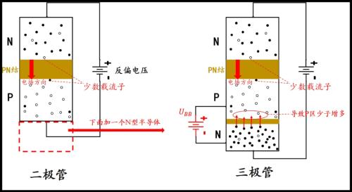
The traditional method is usually divided into three steps, using NPN type as an example (all following discussions are based on example of NPN type silicon tube), as shown in figure below.
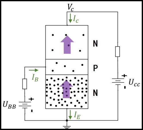
The emitter region injects electrons into base region;
Diffusion and recombination of electrons in base region;
The collector region collects electrons diffused from base region.
Question 1: In this method of explanation in third step, in explaining formation of collector current Ic, no emphasis is placed on explaining reverse bias of collector region from nature of inclusion of carriers, thereby producing Ic, but inappropriately emphasizing high potential effect Vc and at same time emphasizing subtlety of base area. This emphasis is easily misleading. It is believed that as long as Vc is large enough and base area thin enough, collector junction can work in reverse and unidirectional conduction of PN junction will not work. In fact, this just contradicts current principle of amplifying triode. The current triode amplification principle simply requires that Ic and Vc have no value in number in boosted state, and Ic can only be controlled by Ib.
Question 2: The saturation state of a triode cannot be well explained. When triode operates in saturation region, value of Vc is very small or even lower than Vb, and at this time a large reverse saturation current Ic still occurs, that is, when Vc is small, collector junction will still appear reverse conduction is a common phenomenon. This clearly contradicts high potential effect of Vc extraction.
Question 3. The second step of traditional method emphasizes thinness of base region too much, and it is easy to cause such misunderstanding by thinking that base region is thin enough to support reverse direction of triode collector junction. Generally speaking, as long as base region is thin enough, collector junction can lose PN-unidirectional conduction. transition. This clearly contradicts experience that people use unidirectional conductance of two PN junctions inside a triode to judge name of a pin. Even if base area is very thin, when people judge by name of pin, it is not found that unidirectional conduction of PN junction is broken due to thinness of base area. The base area is very thin, but unidirectional conductive characteristics of two PN junctions are still intact, giving people a method and basis for judging triode pin names.
Question 4. When explaining why Ic is controlled by Ib in step 2, and why there is a fixed proportional relationship between Ic and Ib, this cannot be explained visually. This only emphasizes subtlety and low doping of base region from process, but cannot fundamentally explain why current gain remains unchanged.
Question 5: Separation of natural connection between diodes and triodes cannot in principle provide a natural transition along contentnyu. It even gives people conflicting ideas. The diode principle emphasizes that PN junction conducts in one direction and changes cutoff, while triode principle requires that PN junction can conduct in opposite direction. At same time, it cannot reflect historical connection between crystalline triode and electronic triode based on principle of current amplification.

A new way of explaining
01 entry point
If you want to explain a problem in a natural way, you must choose an appropriate entry point. Speaking about principle of triode, let's start with principle of diode. The structure and working principle of diode is very simple, and PN junction inside has unidirectional conduction, as shown in figure.
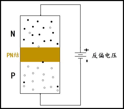
Obviously, diode shown in figure is in reverse bias and PN junction is off. Here, we must pay special attention to shutdown state. In fact, when PN junction is turned off, there will always be a small leakage current, that is, PN junction always has a reverse tripping phenomenon, and PN junction's unidirectional conduction is not 100%.
Why is this happening?
This is mainly due to fact that P region always has a very small number of intrinsic carrier "electrons" in addition to most carrier "holes" created by "doping". The same is true for N region. In addition to majority of carrier electrons, there will also be a very small number of carrier holes.
When a PN junction is reverse biased, most of carriers capable of forward conduction are attracted to power supply, which makes PN junction thicker, and most of carriers can no longer perform function of carrying current through PN. node.
So, at present, formation of leakage current mainly depends on minority carriers, and minority carriers play a conducting role.

As you can see from figure above, internal electric field of PN junction is directed from N region to P region, and this internal electric field facilitates passage of minority carriers through PN junction.
The reason why leakage current is very low is because number of minority carriers is too small. Obviously, magnitude of leakage current at this time mainly depends on number of minority carriers. If you want to artificially increase leakage current, all you have to do is find a way to increase number of minority carriers in reverse bias.
So, as shown in figure, if number of minority carriers can be artificially increased in P or N region, it is natural that leakage current will be artificially increased.
In fact, principle of operation of photodiode is as follows.
The photodiode is same as normal photodiode, its PN junction is unidirectional. Therefore, when photodiode is operating, a reverse voltage should be applied, as shown in figure.
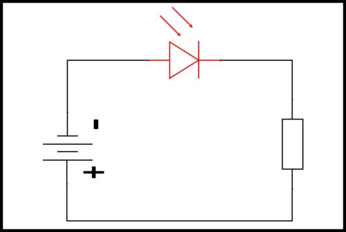
When there is no light, there is also a very small reverse saturation leakage current in circuit, typically 1×10⁻⁸ -1×10 -9A (so-called dark current), which is equivalent to cutting off photodiode at this time;
When there is light, vicinity of PN junction is bombarded with photons, and bound valence electrons in semiconductor absorb energy of photons and are activated to create electron-hole pairs. The amount of these media affects most media. is not large, but for minority carriers in P region and N region, concentration of minority carriers will be greatly increased. Under action of reverse voltage, reverse saturation leakage current will be greatly increased to form a photocurrent. The photocurrent depends on intensity of incident light.
When photocurrent passes through load R, a voltage signal that varies with incident light will be received at both ends of resistor. This is how photodiode completes conversion of electrical function.
The photosensitive diode works in a reverse biased state, because light can increase number of minority carriers, so light will cause reverse leakage current to change, and people use this principle to make photosensitive diode. Since increase in leakage current is artificial at present, increase in leakage current can be easily artificially controlled.
02 emphasizes output
Speaking of this, we should focus on explaining role and properties of primary carrier and non-primary carrier when PN junction is forward-biased and reverse-biased. When it is forward biased, it conducts electricity with majority carriers, and when it is reverse biased, it conducts electricity with minority carriers. Therefore, forward bias current is large, reverse bias current is small, and PN junction exhibits unidirectional electrical properties.
In particular, it should be emphasized that non-primary carriers pass through PN junction in reverse direction very easily during reverse bias, even more easily than primary carriers pass through PN junction in forward direction.
Why?
As we all know, there is an internal electric field created by mutual diffusion of majority carriers inside PN junction, and direction of internal electric field always prevents majority carriers from passing forward. The PN junction must overcome influence of internal electric field, and an external voltage of about 0.7 volts is also required, which is gate voltage for forward conduction of PN junction.
In case of reverse bias, internal electric field will increase under action of power supply, that is, PN junction will thicken. When minority carriers pass through PN junction in opposite direction, direction of internal electric field is consistent with direction of passage of minorx carriers through PN junction, that is, internal electric field at this time will not only not prevent reverse passage of minority carriers, but even contribute to it.
This leads to conclusion we said above: it is very easy for non-primary carriers to pass through PN junction in reverse direction when it is reversed, even easier than for most carriers to pass through PN junction in forward direction. direction.
This conclusion can well explain "problem 2" mentioned above, namely triode saturation state, which will be mentioned in further content of tutorial. In saturation state of triode, collector potential is very low, or even close to or just below base potential, and collector junction is at zero bias, but there will still be a large collector junction reverse current Ic.
03 Natural transition
Continue discussing reverse bias state of a PN junction.
Using light to control amount of minority carriers generated can artificially control amount of leakage current. In this case, people will naturally think about whether control method can be changed, instead of using light to increase minority carriers in N region or P region, in order to realize PN leakage current control. node.management.
That is, instead of "light" method, "electric" method is used to control current (light increases intrinsic carriers, while electrical injection mentioned below increases doped current carriers, intrinsic carriers appear in pairs, which are electron-hole pairs, positive and negative.This is different from doping carriers).
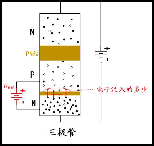
Next, we will focus on P region. The minority carriers in P region are electrons. If you want to inject electrons into P region by electrical injection, it's best to use a dedicated process. N-type semiconductor.
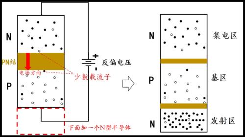
In fact, above image is prototype of NPN transistor, and names and functions of corresponding parts are exactly same as those of transistor.
For convenience of discussion, we directly use names corresponding to triode (for example, "emitter junction", "collector", etc.) for names of various parts shown in figure below.
The electrons in an N-type semiconductor in lowest emitter region exist as a large number of carriers, and as shown in figure, it is very easy to inject or emit electrons from emitter region to P region (base region) Yes, if emitter junction is biased in forward direction.
In particular, it is enough to add a sufficient gate forward voltage (about 0.7 V) between base and emitter. Under action of an external gate voltage, electrons in emitter region will be easily emitted and injected into base region, thus realizing a change in number of "electrons" of minority carriers in base region.
04 IC collector current shaping
After turning on emitter junction with a forward bias voltage, under action of an applied voltage, majority carriers in emitter region - electrons will be easily emitted into base region in large quantities.
Once these media enter base region, their properties in base region (P region) are still of non-base media nature. As previously mentioned, minority carriers can easily pass through reverse biased PN junction in reverse direction, so these electron carriers can easily pass upward through reverse biased collector junction and reach collector. .
It can be seen that formation of collector current does not necessarily depend on high potential of collector. The value of collector current depends more on emission and injection of carriers in emitter region into base region, and depends on degree of such emission and injection. The degree of emission and injection of carriers is in no way related to level of collector potential.
This can naturally explain why collector current Ic has nothing to do with magnitude of collector potential Vc when triode is in expanded state. In boosted state, Ic is not controlled by Vc, and function of Vc is mainly to maintain collector junction reverse-biased to match external circuit conditions required by triode in boosted state.
For Ic, following conclusions can also be drawn: essence of Ic lies in "minority carrier" current, which is an artificially controlled "leakage" current of collector junction, implemented by electron injection, so it can be easily reversed through collector junction. , electrical node.
05 Relationship between Ic and Ib
Following above discussion, collector current Ic has nothing to do with magnitude of collector potential Vc, but mainly depends on degree of carrier injection in emitter region into base region.
It is now clear from above discussion that when triode is in a current amplifying state, main internal current is generated by carrier electrons passing through triode from emitter region to base region and then to collector region. That is, current Ic flowing through triode is basically a flow of electrons.
This through-flow of electrons is very similar to historical electronic triode. The figure below is a schematic diagram of operation of an electronic triode. The current amplification principle of electronic triode can be explained in a natural way thanks to an intuitive understanding of its structure.
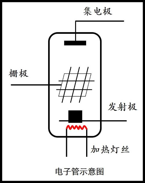
It is easy to understand that fixed proportional relationship between electronic triodes Ib and Ic mainly depends on structure of gate (base) of electron tube.
When conditions of external circuit are met, electronic triode operates in an amplified state. In expanded state, current through tube is basically flow of electrons from emitter to collector through grid. When flow of electrons passes through grid, it is obvious that grid will intercept it, and there is a problem of intercept ratio when intercepting current.
The cutoff factor is mostly related to mesh density. If grid is made dense, its equivalent cutoff area will be larger, and cutoff factor will naturally be larger, and intercepted electron consumption will be larger. Conversely, if intercept ratio is low, less electron flow will be intercepted.
The electron flow intercepted by gate is actually current Ib, and rest of electron flow through gate to collector is Ic. It can be seen from figure that as size of grid structure is determined, cutoff coefficient is also determined, that is, ratio of Ic to Ib is determined.
Thus, as long as internal structure of tube is defined, this ratio is fixed. It can be seen that current gain value β is mainly related to grid density. The denser mesh, larger cutoff factor and lower corresponding β value; sparser grid, smaller cutoff factor and higher corresponding β value.
In fact, current gain ratio of a quartz triode is same as that of an electronic triode.
The base of a quartz triode is equivalent to gate of an electronic triode, and area of the base is equivalent to a grid, but grid of a transistor is dynamic and invisible. In expanded state, when flow of electrons passing through entire tube passes through base region, base region acts similarly to electron tube grid and intercepts flow of electrons (electrons recombine with holes in base region and disappear). when they pass through base zone).
If base region is made thin and doping degree is low, then number of holes in base region will be small, and interception of holes by electrons will be small, which is equivalent to electron tube grid being relatively sparse, flux will be large.
Obviously, if internal structure of transistor triode is determined, cutoff coefficient is also determined. Therefore, in order to obtain greater current gain and make value of β high enough, base region is often made very thin in manufacture of triode, and its doping must be controlled at a very low level.
Unlike a vacuum tube, transistor interception is mainly achieved by neutralizing negatively charged "electrons" in penetrating electron stream with positively charged "holes" distributed in base region.Therefore, current interception effect mainly depends on number of holes in base region.
Moreover, this process is dynamic, "holes" are constantly neutralized by "electrons", and at same time, "holes" are constantly replenished under action of an external power source. During this dynamic process, equivalent total number of holes remains constant. The total number of holes in base region mainly depends on doping degree and thickness of base region. Since structure of transistor is determined, total number of holes in base region will be determined, and corresponding dynamic total will be determined.
This is how cutoff factor is determined, and current gain value of transistor is a fixed value. Therefore, there is a fixed proportional relationship between current Ic and Ib of triode in expanded state.
06 Disable status explanation
The proportional ratio shows that in increased state, current Ic is controlled by current Ib in a fixed ratio, and this fixed control ratio mainly depends on internal structure of transistor.
For a cutoff state where Ib is 0, problem is simplified. When Ib is 0, this means that external voltage Ube is too low and has not reached gate voltage of emitter junction, and in emitter region there is no injection of "electron" carriers into base region, so there will be no current Ib, much less it is impossible to have a current ic.
Also, it's easier to deduce from purely mathematical formula for current amplification, Ic=βIb, Ib is 0, obviously Ic is also 0.

Problems requiring attention in new lecture
Above, we have used new entry angle to discuss principle of triode in explanation method. In particular, it focuses on why collector junction conducts back to form collector current in boosted state of transistor. At same time, it also conducts an in-depth analysis of why current gain of transistor is fixed. value.
The key to this method of explanation is to emphasize connection between diodes and triodes in general.
In fact, it is easy to see from reverse cutoff curve of PN diode that as long as characteristic curve is rotated 180 degrees, as shown in figure, its situation is very similar to output characteristic. triode.
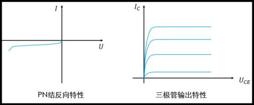
This shows that there is, in principle, an unavoidable connection between a diode and a triode. Therefore, it is very appropriate to choose such an entry point in explain method and start from reverse bias state of PN junction to talk about triode. Moreover, such an explanation will make questions understandable and vivid, and content before and after naturally harmonious and logical.
The disadvantage of this approach is that, starting with PN junction leakage current, it is easy to cause conceptual confusion between intrinsic leakage current and amplified current.
Intrinsic carriers do not contribute to current amplification, and intrinsic carrier current negatively affects transistor performance, which must be overcome. The amplification of current of transistor is mainly achieved by doping carriers. Note conceptual difference.
In addition, it should be noted that, in fact, problem of carriers in a crystal is not simple, it includes analysis of energy level of crystal, energy band structure, and analysis of potential barrier to carrier movement. Therefore, it is not easy to find one or two types of conductors or semiconductors with carriers to make a PN junction or a transistor, and actual process of making a transistor is not so simple.
This kind of explanation method is basically to try to simplify problem as much as possible without violating principles of physics, and try to make it as simple as possible for easy understanding and acceptance. This is the main meaning of this method of explanation.
Related
- This article analyzes in detail principle of triode.
- Leaving aside calculations, in principle workflow of LLC
- Explain in detail classification of more than a dozen types of "recommended collection" capacitors
- Circuit Analysis of 6 Examples Explaining Lightning Surge Protection in Detail
- Explain in detail difference and application of two-three-four-wire system.
- Explain PCB copy process in detail, it's amazing
- The principle of operation and characteristics of relay (relay)
- Sample Analysis! Tell us about the skills of triode amplifier circuitry.
- Understand Current Detection Circuit in One Article
- Principle of electronic switch to realize overcurrent protection
Hot Posts
 How to distinguish induction from leakage, we will teach you three tricks! Ordinary people can also learn super practical
- What is drowning in gold? Why Shen Jin?
- This is a metaphor for EMI/EMS/EMC that can be understood at a glance.
- How many types of pads have you seen in PCB design?
- Summary of Common PCB Repair Techniques
- What is three anti-paint? How to use it correctly?
- Knowing these rules, you will not get confused looking at circuit diagram.
- How to make anti-interference PCB design?
- Can diodes do this?