Location:Home Page > Archive Archive
Explain PCB copy process in detail, it's amazing
2023-03-18【Archive】
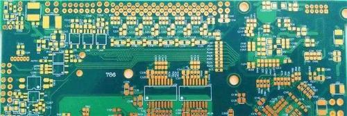
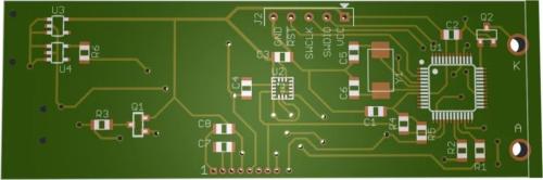
The technical process for implementing a copy PCB board is to simply scan PCB for copying, record detailed location of components, and then remove components to make a BOM and organize material procurement. scanned to an image and restored to a PCB drawing file by copying board software, and then PCB file is sent to plate factory to make board. .
01
Specific production steps for PCB replication
1. Get PCB, first write down model, parameters and position of all components on paper, especially direction of diode, triode and IC cutout direction. It is best to take two pictures of location of vital parts with a digital camera. Modern printed circuit boards are becoming more and more sophisticated, and some of diodes and triodes on them are not visible unless you pay attention.
2. Remove all parts of multilayer board and remove tin from PAD hole. Clean circuit board with alcohol, and then place it in scanner. The scanner should enlarge scan pixels a little to get a sharper image. Then lightly buff top layer and bottom layer with gauze paper until copper film is shiny, place it in scanner, start PHOTOSHOP and scan two layers separately in color. Please note that printed circuit board must be placed horizontally and vertically in scanner, otherwise scanned image cannot be used.
3. Adjust contrast and brightness of canvas so that contrast between part with copper film and part without copper film is strong, then convert next image to black and white, check if lines are clear, if not, repeat this step. If it is clear, save image as black and white BMP format files TOP.BMP and BOT.BMP. If you find any problem with image, you can use PHOTOSHOP to correct and fix it.
4. Convert two BMP files to PROTEL files respectively and transfer two layers to PROTEL. If positions of PAD and VIA mostly overlap after two layers, this indicates that previous steps have been performed well. If there is a deviation, repeat third step. Therefore, PCB copying board is a job that requires patience, because a small problem will affect quality and degree of conformity after board is copied.
5. Convert BMP of top layer to TOP.PCB, note conversion to SILK layer which is yellow layer, and then you just draw a line on top layer and place device according to drawing in second step. Oudacast SILK layer after drawing. Repeat until all layers are drawn.
6. Import TOP.PCB and BOT.PCB into PROTEL and merge them into one image.
7. Use a laser printer to print TOP LAYER and BOTTOM LAYER on a transparent film (1:1 ratio), place film on PCB and compare if there are any errors. If it's right, you're done.
A copy of original board is created, but that's only half battle. It is also necessary to check if electronic specifications of copy board are same as those of original board. If it's same, then it's really done.
Notes: If this is a multi-layer board, it must be carefully sanded down to inner layer, while repeating steps three through five of copying board. Of course, graphics names are different too, depending on layer. Depending on number, a generic double-sided copy board is much simpler than a multi-layer board (vias are prone to problems).
02
Double-panel copyboard method
1. Scan top and bottom of PCB and save two images in BMP format.
2. Open Quickpcb2005 board copy program, click "File" and "Open Basemap" to open scanned image. Use PAGEUP to enlarge screen, see pad, press PP to place pad, see line and press PT to route... Just like a child traces an image, draw it once in this program and press " Save" to create B2P file.
3. Then click "File" and "Open Basemap" to open scanned color map of another layer.
4. Then click "File" and "Open" to open previously saved B2P file, we can see board we just copied stacked on top of this image - same PCB board, hole is in same place, just wiring is different. So we click Options - Layer Settings, here we turn off lines and silkscreen showing top layer, leaving only layered vias.
5. The vias on top layer are in same position as vias on image of bottom layer. Now we can draw bottom line in same way as we did in childhood. Then click Save - B2P file now has a top and bottom data layer.
6. Click "File" and "Export as Board File" and you can get a board file with two levels of information that can be re-edited or reproduced with a schematic diagram or directly sent to board. slab plant for production.
03
Multilayer Board Copy Method
Actually, copying a 4-layer board means copying two double-sided boards repeatedly, and copying a six-layer board means copying three double-sided boards repeatedly... you can't see internal wiring. How can we see inner layer of a complex multilayer board? - stratification.
There are many layering methods, such as Corrosion Potion, Knife Scraping, etc., but it's easy to layer and lose data. Experience tells us that grinding is most accurate.
When we finish copying top and bottom layers of PCB, we usually use sandpaper to polish surface to expose inner layer; Rub board evenly (if board is small, you can also smooth out sandpaper by holding PCB with one finger and rubbing it with sandpaper). The point is to lay it flat so that it can be sanded evenly.
Silkscreen and green oil are usually washable, and copper wire and copper skin need to be wiped several times. Generally speaking, a bluetooth board can be wiped in a few minutes, and a flash drive in about ten minutes, of course, if power is strong, it will take less time, if power is small, then it will take a little more time.
The sanding plate is currently most common layering solution and also most economical. We can find a defective board and try it. Actually, there is no technical difficulty in grinding board, but it is a bit boring and requires little effort. Don't worry about grinding board through and chafing with your fingers.
During PCB layout process, after system layout is completed, PCB layout should be reviewed to ensure that system layout is reasonable and can provide best effect.
This can usually be explored in following ways:
1. Does layout of system provide reasonable or optimal wiring, can it provide reliable wiring, and can it ensure that circuit operates reliably. When laying, it is necessary to have a general idea and plan for direction of signal and power and ground network.
2. Whether size of PCB matches size of machining drawing, whether it meets requirements of PCB manufacturing process, and whether there is a behavioral mark. This point requires special attention. The circuit and layout of many PCBs are designed beautifully and intelligently, but exact location of positioning connectors is neglected, as a result, circuit design cannot be docked with other circuits.
3. Whether components conflict in 2D or 3D space. Pay attention to physical dimensions of device, especially its height. When soldering components without layout, height usually cannot exceed 3mm.
4. Whether layout of components is tight and orderly, whether they are neatly arranged, and whether they are all finished. When laying out components, consider not only direction of signal and type of signal, areas that require attention or protection, but also overall density of arrangement of devices to achieve uniform density.
5. Is it easy to replace components that need to be replaced frequently, and is it easy to insert a replacement board into equipment. The convenience and reliability of replacement and installation of frequently replaced components must be ensured.
Related
- Explain PCB copy process in detail, it's amazing
- Explain in detail difference and application of two-three-four-wire system.
- Explain in detail classification of more than a dozen types of "recommended collection" capacitors
- PCB design guidelines: safety regulations, layout and wiring, EMC, thermal design, process engineering.
- Circuit Analysis of 6 Examples Explaining Lightning Surge Protection in Detail
- What does inside of a multilayer PCB look like? Three-dimensional general analysis of design process of high-quality printed circuit boards
- How many types of pads have you seen in PCB design?
- Do you know layout requirements of some special devices in PCB design?
- In PCB industry, we all need to know these 5 important common sense rules.
- Finally, it becomes clear that process of obtaining switching losses of a MOSFET in a switching power supply
Hot Posts
 How to distinguish induction from leakage, we will teach you three tricks! Ordinary people can also learn super practical
- What is drowning in gold? Why Shen Jin?
- This is a metaphor for EMI/EMS/EMC that can be understood at a glance.
- How many types of pads have you seen in PCB design?
- Summary of Common PCB Repair Techniques
- What is three anti-paint? How to use it correctly?
- Knowing these rules, you will not get confused looking at circuit diagram.
- How to make anti-interference PCB design?
- Can diodes do this?