Location:Home Page > Archive Archive
Six common design schemes for current measurement circuits
2023-11-27【Archive】
Design diagram of current detection circuit (1)
The current sense resistor of current sense circuit on low voltage side is connected in series with ground (Figure 1), and current sense resistor of current sense circuit on high voltage side is connected in series with ground (Figure 1). high voltage terminal (fig. 2). Both methods have their own characteristics: low side current method adds an additional wire resistor to ground loop, while high side current method must deal with a large common mode signal.
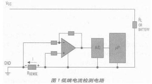
The low-side current-sense op-amp shown in Figure 1 uses ground as its reference level, and a current-sense resistor is connected to positive phase terminal. Common mode range at op amp input: (GNDRSENSE*ILOAD). Although LV side current sensing circuit is relatively simple, there are several fault conditions that LV side current sensing circuit cannot detect, which can lead to a dangerous situation for load. solve these problems.
A high-end current detection circuit is directly connected to power supply terminal, which can detect any fault in downstream circuit and take appropriate protection measures, especially suitable for automatic control applications, since chassis is usually used as a reference. ground in these application circuits.
Design diagram of current detection circuit (2)
There are many implementations of traditional high/low side current measurement methods, most of which are based on circuits with discrete or semi-discrete components. A high quality current measurement circuit usually requires a precision op amp and some precision resistors and capacitors. The most commonly used high performance current measurement circuit uses a differential op amp to amplify gain and shifts signal from high frequency to reference ground (Figure 3):

VO=IRS*RS;R1=R2=R3=R4
This scheme has been widely used in practical systems, but this scheme has three major drawbacks:
1) The input impedance is relatively low, equal to R1;
2) The input resistance of input terminal usually has a large error value;
3) Resistor matching is necessary to provide acceptable CMRR. A 1% change in any resistor will bring CMRR down to 46dB, a 0.1% change will bring CMRR to 66dB, and a 0.01% change will bring CMRR down to 46dB. CMRR Up to 86dB High-quality current detection requires high measurement skills, which contributes to development of high-quality current detection integrated circuits. And current measurement technology on underside does not seem to have corresponding progress.
Design diagram of current detection circuit (3)
Using built-in differential op-amp to detect high-side current
Circuits using differential op amps to measure current on high side are easier to use because of many recently introduced integrated circuits. The integrated circuit includes a precision op-amp and well-matched resistors, and CMRR reaches approximately 105 dB. One such product is MAX4198/99, which has a 110dB CMRR, better than 0.01% gain error, and comes in a small 8-pin mMAX package.
The special high-side current detection circuit contains all functional blocks for high-side current detection. It can detect high-side current at up to 32V common-mode voltage, and provide a current proportional to ground level as a reference point. This approach is suitable for applications requiring accurate current measurement and control, such as power management and battery monitoring.
The current sense resistor used in MAXIM high performance current sense op amp is placed between RF power supply and input terminal of circuit to be detected. High-end technology without adding extra impedance to ground loop improves overall circuit performance and simplifies layout requirements.
MAXIM has launched a series of bi-directional or uni-directional current detection ICs. Some bi-directional current detection ICs have built-in current detection resistors that can sense amount of current flowing into or out of circuit under test and display direction of current through polarity-indicating pin. Variable Gain Current IC, Fixed Gain Current IC (+20V/V, +50V/V, or +100V/V) or Fixed Gain Current IC including single and dual comparators, all in a compact package - bulky packages such as SOT23 for size-critical applications. On fig. 4 shows current detection circuit on side youhigh voltage, consisting of MAX4173.
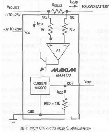
The relationship between output voltage and measuring resistor in figure is as follows:
o=RGD*(Iload*Rsense)/RG1)
*b, where b is mirror current factor
The above formula can be simplified as follows:
Vo=“Gain”*Rsense*Iload;Gain= b*RGD/RG1
Gain: 20 (MAX4173T), 50 (MAX4173F), 100 (MAX4173H).
It can be seen from above calculation formula that CMRR is determined by process of internal integrated current detection circuit (typical value > 90 dB) and is no longer dependent on external resistance.
Using built-in current detection circuit has following advantages:
1. Device stability is good
2. Excellent temperature drift performance
3. Small size
4. Low power consumption
5. Ease of use
Precautions when choosing a current sense resistor
The RSENSE current detection resistor should be selected according to following principles:
1. Loss of voltage: if resistance value of current sense resistor is too high, power supply voltage will decrease by value of IR. To reduce voltage losses, you should choose a current sense resistor with a small resistance value.
2. Accuracy: Larger current sense resistors can provide better accuracy for small current measurements. This is because greater voltage across sensing resistor, less will be effect of op-amp bias voltage and input bias current.
3. Efficiency and Power Consumption: At high current, power consumption of I2R on RSENSE cannot be ignored. This must be kept in mind when considering sense resistor and power dissipation. If sensing resistor is allowed to heat up, value of resistor may be larger.
4. Inductance: If ISENSE contains many high frequency components, inductance of sensing resistor should be small. Wirewound resistors have highest inductance, while metal film resistors are better.
5. Cost: If price of a suitable current sense resistor is too high, another alternative can be used (Figure 5). It uses PCB traces as a current sense resistor. Since "resistance" of PCB copper wire is not accurate, a potentiometer is needed in circuit to adjust total current value. In addition, temperature drift of copper wire is relatively large (about 0.4%/°C), which must be taken into account in systems operating over a wide temperature range.

Design diagram of current detection circuit (4)
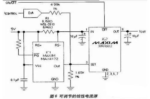
A variable linear current source (Figure 6) is a typical application circuit consisting of a high quality current detector. IC1 converts current of resistor R1 into a corresponding proportional voltage signal and controls voltage regulator IC IC2 to produce a stable output signal. DAC current can provide digital control of IOUT. To meet 12-bit (60mA LSB) accuracy requirement, you can use MAX530 parallel interface or MAX531 serial interface. For 10-bit accuracy (250mA LSB), you can use MAX503 parallel interface or MAX504 serial interface.
Design diagram of current detection circuit (5)
Modeling devices of voltage and current recording system based on microcontroller 51
This design uses AT89C51 as main control chip, and ADC0804 is used as external voltage measurement chip. The external voltage is up to 10V, and maximum voltage of ADC0804 is +5V. The test voltage is divided by half of original, so that detected voltage becomes 0-5V from 0-10V, which meets input requirements of ADC chip. With 2, previous measured voltage can be restored.
The voltage alarm circuit consists of a relay, an LED and an audible signal. When voltage detected by ADC chip exceeds a certain limit, specific I/O port will go low, PNP transistor will be turned on, relay will be turned on, and LED and speaker will form a voltage drop. An alarm is generated.
The voltage value collected by ADC chip and current value converted and calculated from resistance are displayed on LCD.
The alarm voltage is set by two buttons. Pressing button once increases alarm value by 0.1V, and pressing button twice subtracts alarm value by 0.1V.
By comparing data acquisition voltage with alarm voltage, at any time inside chip, when data acquisition voltage is higher than alarm voltage, an alarm is activated.
General circuit diagram
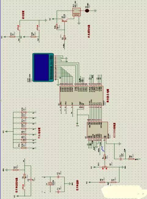
Simulation graphics
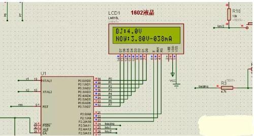
Scheme for displaying voltage, current
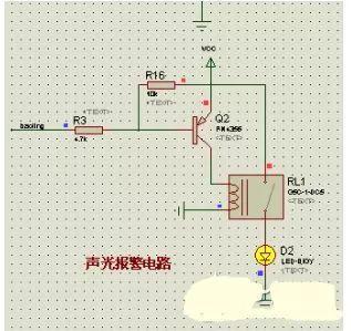
Scheme of sound and light signaling
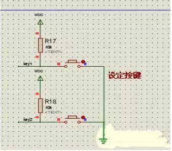
Key setting scheme
This design is extremely complex as 12864 only has an LCD without a font library. Due to timing issues. The software only debugs LCD 1602 display. I believe that while there is time, the 12864 display will be completed.
Design diagram of current detection circuit (6)
A current measurement amplifier with a wide common-mode range. The MAX44284 current-sensing amplifier combines high accuracy with a wide common-mode input range. You get high accuracy and low power consumption, all in Maxim's signature minimalist design. This device sets a new standard for current-sensing amplifiers with high accuracy, high flexibility, and excellent value for money, making it ideal for medical, consumer electronics, mobile, communications, or motor control applications - any application that requires high accuracy and lightness. design.
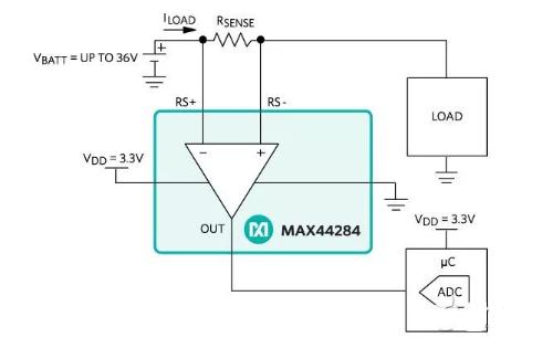

Excellent accuracy
2µV input offset, only 0.05% gain error
Extremely low input offset temperature coefficient: 50 nV/°C
Wide -0.1V to +36V common-mode input range
Low offset drift and input noise
Provides shutdown control to conserve battery power
Related
- Six common design schemes for current measurement circuits
- Six Methods for Testing PCB Short Circuits
- A little knowledge of power circuits: will help you understand difference between source current and drain current.
- Analysis and application of four common DC power supply circuits
- must read! Electronics Engineers Must Master 7 Common Interfaces in Circuits
- 50 Common Hardware Design Patterns
- Commonly Used Diode Circuits Essential for Engineers
- Explain in detail difference between analog and digital circuits in PCB design.
- Three common grounding methods in circuit design
- In circuit design, what are differences between six types of grounds?
Hot Posts
 How to distinguish induction from leakage, we will teach you three tricks! Ordinary people can also learn super practical
- What is drowning in gold? Why Shen Jin?
- This is a metaphor for EMI/EMS/EMC that can be understood at a glance.
- How many types of pads have you seen in PCB design?
- Summary of Common PCB Repair Techniques
- What is three anti-paint? How to use it correctly?
- Knowing these rules, you will not get confused looking at circuit diagram.
- How to make anti-interference PCB design?
- Can diodes do this?