Location:Home Page > Archive Archive
Finally, it becomes clear that process of obtaining switching losses of a MOSFET in a switching power supply
2023-05-04【Archive】
Power supply engineers know that MOS switching loss factor in entire power system is not small. We are talking about MOS switching loss, most of all it is turn-on loss and turn-off loss, because these two losses are not like conduction loss. This is as intuitive as pass loss or drive loss, so some people are still a little confused about it calculation.
Today, we're using reverse CCM turn-on and turn-off loss to come up with a formula that we hope will inspire you.
We know that these losses are due to crossover losses caused by crossing voltage and current at a very short turn-on or turn-off moment, so we must first draw crossover curve and then step by step. waveform step Step-by-step derivation of formula for its calculation.
Let's look at picture together. The picture below shows process of superposition of current and voltage during switching. This picture describes worst situation. When current rises to I1 when mos tube is turned on, mos voltage does not start. It starts to drop, and mos tube current starts to drop after voltage on mos tube rises to Vds when it is turned off.
Worst case analysis:
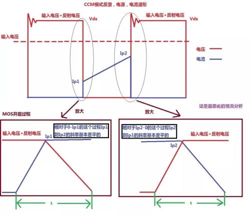
mos tube opening process
Phase 1: voltage constant and current rising (voltage constant Vds and current increasing from 0 to Ip1). At moment mos is turned on, current rapidly increases from zero to Ip1, and DC MOS does not change voltage by Vds;
Phase 2: current is constant and voltage drops (Ip1 current is constant and voltage drops from Vds to 0). current at this time (section Ip1-Ip2) Compared to 0-Ip1 moment, it is very slow. -transistor starts dropping rapidly to 0V.
Mos Tube shutdown process
Phase 1: current is constant and voltage rises (current Ip2 is constant and voltage rises from 0 to Vds). The voltage quickly begins to rise from 0 to maximum voltage. Vds, which is same as opening MOS. The current basically does not change on Ip2;
Phase 2: voltage is constant and current drops (spot voltage Vds is constant and current drops from Ip2 to 0). At this time, voltage Vds is constant and current drops rapidly from Ip2 with a large value. The slope drops to 0.
The worst-case switching situation is discussed above, but in my personal experience, this is just a misunderstanding. I have not come across such a situation, so I don't usually use such a situation to calculate switching losses.
Because I don't use it myself, I won't draw a detailed conclusion for situation described above. The worst-case turn-on and turn-off loss calculation formula is directly given below.
With regard to transition time t off and on, evaluation process will be given below.
Personally, I think that analysis and conclusions are more consistent with real situation, see picture.
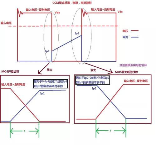
The difference between this situation and previous one is this:
On power-up: The process of rising current 0-Ip1 and process of falling voltage Vds-0 occur simultaneously.
Turn-off stage: The 0-Vds voltage rise process and current fall process from Ip2-0 occur simultaneously.
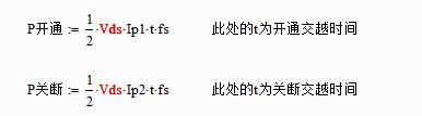
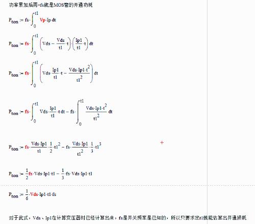
Turn-on losses
Let's first find traffic opening time at time t1
It seems that we can use average method to directly calculate, Ip1/2 × Vds/2 *t1*fs, actually this is wrong, actual exact calculation of this process is that during time t Each instant corresponds to power, and then accumulate all instantaneous power for this period and then divide it by switching period T or multiply it by switching frequency fs. Well, when we have an idea, there are only math problems left, let's see together.
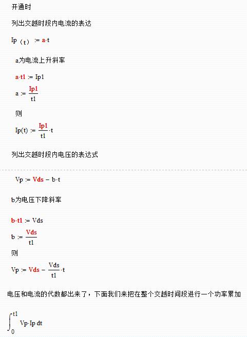
Let me talk about t1 estimation method.
The idea is to calculate time t1 according to total gate charge given in MOSFET datasheet and use formula Qg=i*t to calculate.
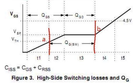
Let's take a look at arousal process in figure above. Vth is turn-on threshold of MOS lamp, and Vsp is Miller platform of MOS lamp. In fact, process from beginning of MOS tube to saturated conduction is from control voltage from point to point b in this interval.
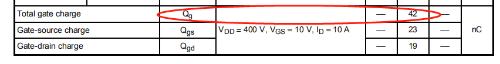
The total gate charge Gg can be found in mos tube datasheet.
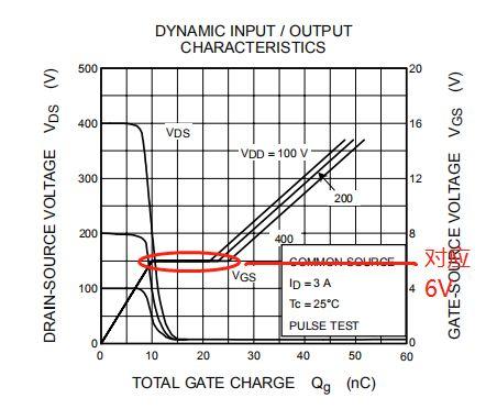
Then this is field current required during this period, let's look at figure below, value of this current is combined with your actual field circuit.

The current i can be calculated according to value of resistor R1 and Miller plateau voltage.
Miller plateau voltage Vsp can also be found in MOS lamp datasheet.
Then, according to your actual supply voltage (in fact, it is approximately equal to Vcc supply voltage of chip), before actual voltage is created, you can preset it in theoretical evaluation stage, for example, preset 15 V.
When calculating, we consider section from Vth to Vsp to be approximately equal to Vsp, and then it is easy to calculate i. i=(Vcc-Vsp)/R1, excitation current i was calculated at this point, and then platform time (from point a to point b) t1 was calculated. Qg=i*t1, t1=Qg/i, now almost same. So, let's summarize formula for calculating turn-on loss of MOS switch, i=(Vcc-Vsp)/R1, calculate control current at pad t1=Qg/i, and calculate duration of pad operation (i.e. when MOS is on, voltage and current ) Pon=1/6*Vds*Ip1*t1*fs.
Losses during outage
There is no difference between calculation of turn-off losses and method of outputting turn-on losses, I will not repeat here, I will give a simple result.
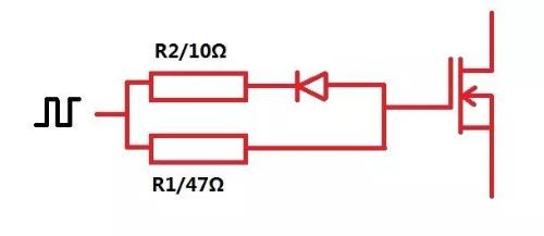
i=(Vsp)/R2, calculate platform drive current. t1=Qg/i, calculate platform duration (i.e. voltage and current crossing time when MOS is turned off) Ptoff=1/6*Vds*Ip1*t1*fs.
The above is for flyback CCM, calculation method for DCM is same, but for DCM, Ip1 is 0, turn-on loss is negligible, and calculation method for turn-off loss is same.
Related
- Finally, it becomes clear that process of obtaining switching losses of a MOSFET in a switching power supply
- Analysis of various losses inside a switching power supply from 4 aspects
- Analysis of damping RC circuit of a switching power supply "haberdashery"
- Detailed analysis of the "various protection schemes" of a switching power supply
- Engineer Daniel tells you: The "Y Capacitor" of a switching power supply is calculated in this way.
- Four ways to reduce the output "ripple and noise" of a switching power supply
- Various losses inside switching power supply
- Do not underestimate "form of high-frequency magnetic core" in switching power supply, what effect does it have on transformer?
- Notes on whole switching power supply design process!
- The best switching circuit design process for power supplies is a must for engineers!
Hot Posts
 How to distinguish induction from leakage, we will teach you three tricks! Ordinary people can also learn super practical
- What is drowning in gold? Why Shen Jin?
- This is a metaphor for EMI/EMS/EMC that can be understood at a glance.
- How many types of pads have you seen in PCB design?
- Summary of Common PCB Repair Techniques
- What is three anti-paint? How to use it correctly?
- Knowing these rules, you will not get confused looking at circuit diagram.
- How to make anti-interference PCB design?
- Can diodes do this?