Location:Home Page > Archive Archive
Notes on whole switching power supply design process!
2023-03-18【Archive】
Part 1Overview
Designing a switching power supply is a time-consuming and time-consuming task, requiring many design parameters to be constantly changed until performance is up to task. This article describes design steps for a flyback converter step by step, and takes design of an isolated flyback converter with two 6.5W outputs as an example. The main control chip uses NCP1015.
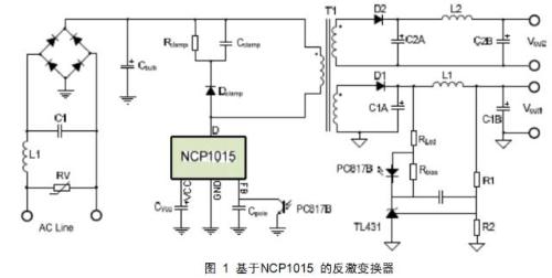
A basic flyback converter is shown in Figure 1. A flyback converter (flyback converter) is most often used in low-power (1-60 W) switching power supplies that require galvanic isolation of input and output Topology (Topology). Simplicity, reliability, low cost and ease of implementation are outstanding advantages of flyback converter.
Part 2Design steps
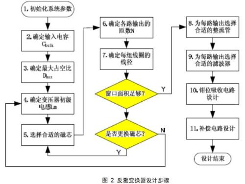
Next, refer to design steps shown in fig. 2 to design flyback converter step by step
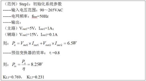
Step 1. Initialize system settings
------Input voltage range: Vinmin_AC and Vinmax_AC
------network frequency: fline (internal frequency 50 Hz)
------output power: (equal to sum of output power of each channel)

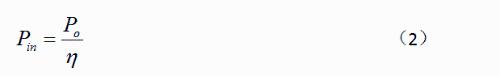
------ Preliminary estimation of inverter efficiency: η (at low output voltage, η is 0.7~0.75, at high output voltage, η is 0.8~0.85) According to the calculated Efficiency rate input power:
For multiple outputs, define KL(n) as ratio of nth output power to total output power:
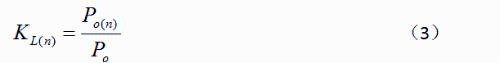
For one output KL(n)=1.
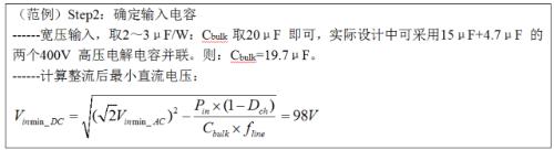
Step 2. Determine input capacitance Cbulk
The value of Cbulk depends on input power. Generally, wide input voltage range (85-265VAC) is 2-3µF/W, narrow input voltage range (176-265VAC) is 1µF/W. Tue The charge fill factor Dch is typically 0.2.
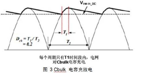
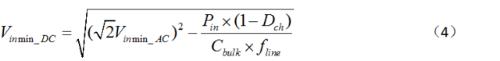
Typically, flyback converter is designed for minimum Vinmin_DC voltage after rectification, and Vinmin_DC can be calculated using Cbulk:
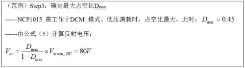
Step 3. Determine maximum duty cycle Dmax
The flyback converter has two modes of operation: continuous inductor current mode (CCM) and discontinuous inductor current mode (DCM). Both modes have their advantages and disadvantages, relatively speaking, DCM mode has better switching characteristics, and secondary rectifier diode turns off at zero current, so there is no diode reverse recovery problem in CCM mode. In addition, at same power level, since transformer in DCM mode stores less energy than in CCM mode, size of transformer in DCM mode is smaller. However, compared to CCM mode, DCM mode increases RMS value of primary current, which increases conduction loss of MOSFET and increases current load of secondary output capacitor. Therefore, CCM mode is often recommended for low voltage, high current output cases, and DCM mode is often recommended for high voltage, low current output cases.
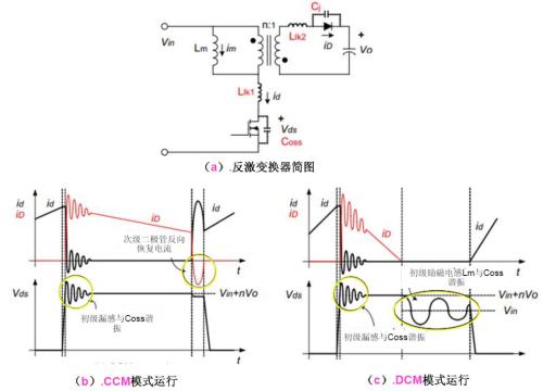
Fig. 4. Flyback Converter
For a flyback converter in CCM mode, input/output voltage gain is determined by duty cycle only. In a DCM flyback converter, input/output voltage gain is determined by both duty cycle and load conditions, which adds complexity to DCM circuitry. However, if we design a DCM flyback converter at critical point between DCM mode and CCM mode (BCM mode), lowest input voltage (Vinmin_DC) and full load conditions, problem can be simplified. Thus, whether flyback converter operates in CCM mode or DCM mode, we can design it according to CCM mode.
As shown in Figure 4(b), when MOSFET is turned off, input voltage Vin and secondary reflected voltage nVo are superimposed on both ends of DCF of MOSFET. After determining maximum duty cycle Dmax, reflected voltage Vor (i.e. nVo), maximum voltage VD sensed by secondary rectifier diode, and maximum voltage Vdsmax sensed by MOS lamp can be obtained from following formula:
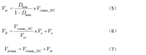
From formulas (5) (6) (7), it can be seen that smaller value of Dmax, smaller Vor and smaller voltage of MOS tube, but voltage of secondary tube of rectifier increases. Therefore, we must increase Dmax as much as possible to reduce voltage of secondary rectifier lamp, provided that there is sufficient margin of MOS lamp. The value of Dmax should ensure that Vdsmax does not exceed 80% of rated withstand voltage of MOS lamp, at same time, for a flyback converter controlled in peak current mode, under CCM conditions, when duty cycle exceeds 0.5, a subharmonic shock will occur. Considering in complex, for a MOS lamp with a withstand voltage value of 700V (NCP1015), it is advisable that in design Dmax does not exceed 0.45.
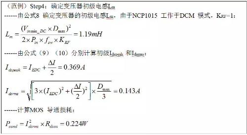
Step 4. Determine transformer's primary inductance Lm
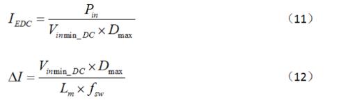
For reverse operation in CCM mode, when input voltage changes, converter can switch from CCM mode to DCM mode, for both modes, primary inductance of transformer is designed for worst conditions (lowest input voltage, full load) Lm . Defined by:
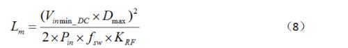
Among them, fsw is operating frequency of flyback converter, KRF is current ripple factor, and its definition is shown in the figure below:
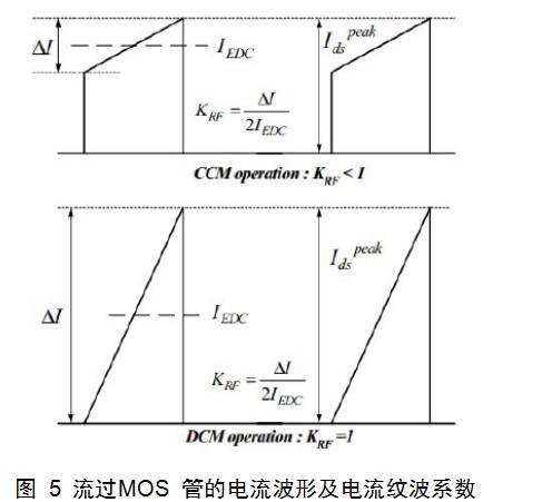
For DCM mode converter, KRF=1 at design time. For CCM mode converter, KRF<1, at this time, KRF value will affect RMS value of primary current. The smaller KRF, smaller RMS value and smaller loss of MOS tube. design. Generally speaking, when designing a flyback converter in CCM mode, wide voltage input (90-265VAC) KRF is 0.25-0.5, narrow voltage input (176-265VAC) KRF is 0.4- 0.8.
Once Lm is determined, peak current Idspeak and RMS value Idsrms of current flowing through MOS tube are also determined:
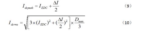
Where:
The design must ensure that Idspeak does not exceed 80% of maximum current of selected MOS lamp. MOS tube resistance.

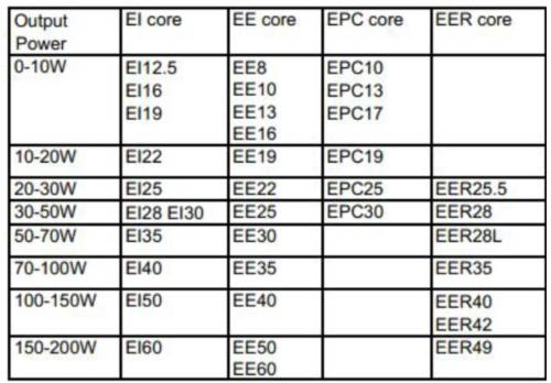
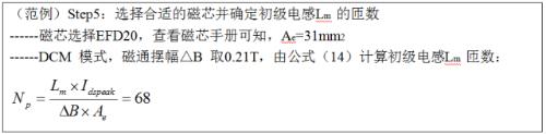
Step 5. Select appropriate magnetic circuit and number of turns of transformer primary inductance
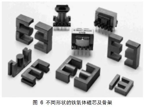
In design of switching power supplies, ferrite core is most widely used core, which can be shaped into various shapes to meet different application requirements, such as multiple outputs, physical height, cost optimization, etc.
In a real design, due to too many variables, choice of magnetic core is not very strictly limited, and there are many possibilities to choose from. One of selection methods is that we can refer to selection guide provided by magnetic core supplier for selection. If there is no suitable link, you can refer to following table:
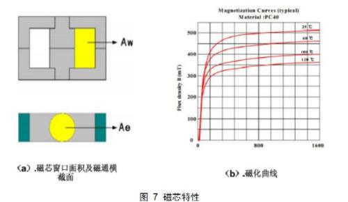
Once core is selected, look up Ae value and magnetization curve in its datasheet to determine flux swing △B, and number of turns of secondary coil is given by following formula:
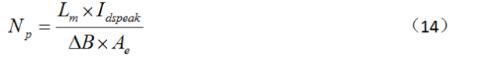
Among them, in DCM mode, △B is 0.2~0.26T, and in CCM △B is 0.12~0.18T.
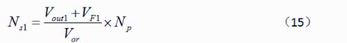
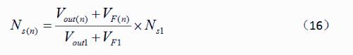
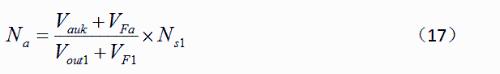
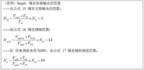
Step 6. Determine number of turns for each output
First, number of turns of feedback winding of main circuit is determined, and number of turns of other windings can be based on number of turns of main circuit winding. Number of turns of main winding of feedback loop:
Then number of turns of remaining output windings is:
The number of turns Na of auxiliary winding of coil is:
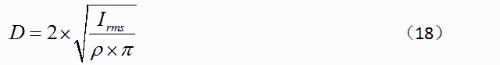
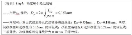
Step 7. Determine wire diameter of each winding
Determine winding wire diameter according to RMS current flowing through each winding.
effective current of primary winding of inductor:

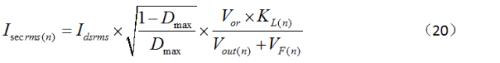
The effective value of current of secondary winding is determined by following formula:
ρ - current density, unit: A/mm2, usually with a relatively long winding coil (>1 m), coil current density is 5 A/mm2, with a short winding coil, coil current density is 6~ 10A/mm2. When current flowing through coil is relatively large, several sets of thin wires can be wound in parallel to reduce influence of skin effect.
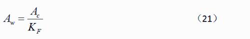
Among them, Ac is sum of cross-sectional areas of all winding wires, and KF is fill factor, which is usually 0.2 to 0.3.
Check area of the magnetic circuit window (as shown in Figure 7(a)), it must be larger than result calculated by formula 21.
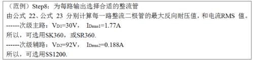
Step 8. Select correct rectifier for each output
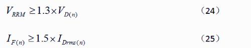
The maximum reverse voltage VD(n) and RMS value IDrms(n) of output rectifier tube of each winding are as follows:
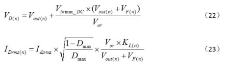
The reverse withstand voltage value and rated forward conduction current of selected diode must meet following requirements:
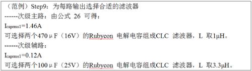
Step 9. Choose an appropriate filter for each output
The ripple current Icaprms(n) of nth output capacitor Cout(n) is:

The value of ripple current Iripple of selected output capacitor must match:

Output voltage ripple is determined by following formula:
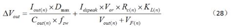
Sometimes high ESR of a single capacitor makes it difficult for inverter to achieve desired low ripple performance. At this time, we can connect several capacitors in parallel at output, or add an LC filter. To improve ripple noise of converter. Note: The corner frequency of LC filter should be greater than 1/3 of switching frequency. Given that switching power supply may have a capacitive load in practical applications, L should not be too large, and it is recommended not to exceed 4.7 µH.
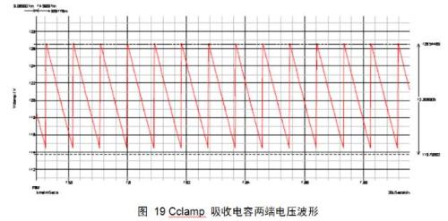
Step 10 Designing Damping Clamp Circuit
As shown in Figure 8, when MOSFET is turned off in flyback converter, resonant peak caused by leakage inductance of LLK transformer and output capacitance of MOSFET is added to drain of MOSFET. there is no limit, life expectancy of MOS tube will be greatly reduced. Therefore, measures must be taken to absorb this surge.
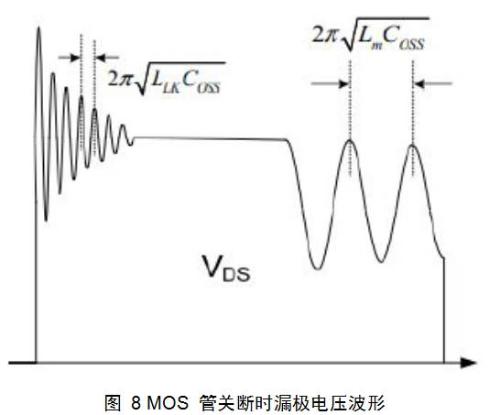
In design of flyback converter, circuit shown in fig. 9(a) is commonly used as a soak-clamp (RCD clamp) circuit of a flyback converter.
RClamp is defined by following formula, where Vclamp is typically 50-100V higher than reflected voltage Vor and LLK is primary leakage inductance of transformer to be actually measured:
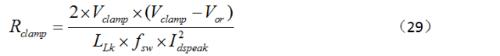
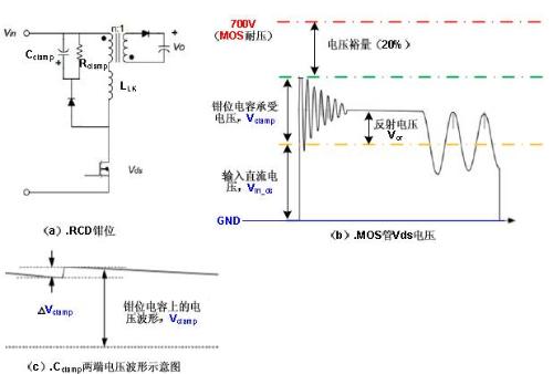
Fig. 9. RCD clamp absorption
CClamp is determined by following formula, where Vripple is usually between 5% and 10% of Vclamp, which is more reasonable:
When output power is relatively small (less than 20W), clamping diode can be a slow recovery diode, such as 1N4007; otherwise, a fast recovery diode is required.

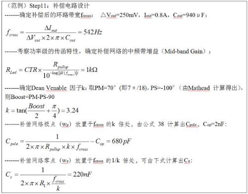
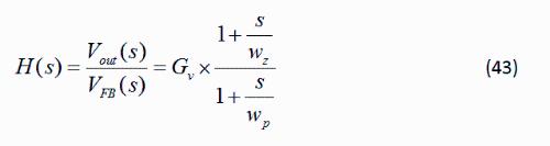
Step 11. Designing Compensation Scheme
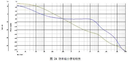
Switched-mode power supply system is a typical closed loop control system, when designing, debugging compensation circuit takes a significant workload. Most of currently popular flyback controllers on market use peak current control mode. The weak signal of peak current reverse mode power stage can be simplified as a first order system, so its compensation circuit is easy to design. It is usually sufficient to use type II compensation scheme proposed by Dean Venable.
Before designing a compensation circuit, you must first study weak signal characteristics of compensation object (power stage).
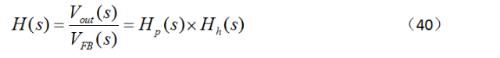
As shown in Figure 8, if inverting pin of IC's internal comparator is disabled, transfer function from control to output (that is, transfer function of the control object):
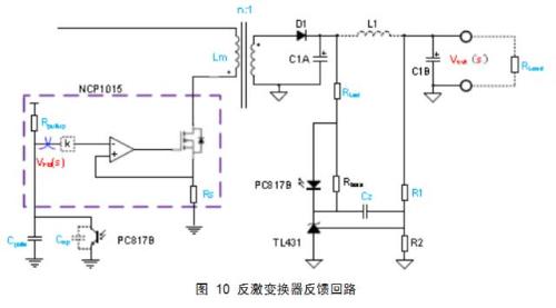
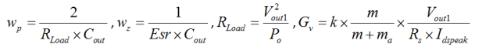
The appendix shows transfer function models of power stage in CCM mode and flyback converter in DCM mode, respectively. NCP1015 works in DCM mode, transfer from control to output:
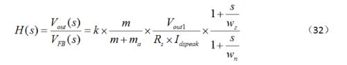
Where:
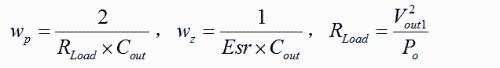
Vout1 outputs DC voltage for main circuit, k is damping factor from error amplifier output to current comparator input (for NCP1015, k=0.25), m is primary current slope, and ma is slope compensation slope (because there is no slope compensation inside NCP1015, i.e. ma=0), Idspeak is primary peak current under given conditions. So we can use Mathcad (or Matlab) to draw Bode diagram of power level transfer function:
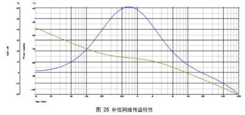
By examining Bode diagram of power stage transfer function, we can perform loop compensation.
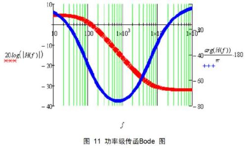
As mentioned above, for a flyback converter in peak current mode, use a Dean Venable type II compensation circuit. A typical connection method is shown in figure below:
Typically, to reduce ripple noise at output, a small LC filter is added to output, as shown in Figure 10. The second-order low-pass filter, consisting of L1 and C1B, affects stability of output signal. loop, L1 , Introduction C1B complicates analysis of converter loop, which affects not only transfer characteristics of power stage, but also transfer characteristics of compensation network. However, after analyzing simulation, it can be seen that if corner frequency L1 and C1B is more than 5 times bandwidth fcross, then its effect on loop can be neglected. In a real design, it is recommended that L1 does not exceed 4.7. µH. Therefore, when we simplify analysis, we simply close L1 directly and get transfer function G(s) of compensation network as:
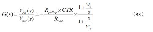
Where:
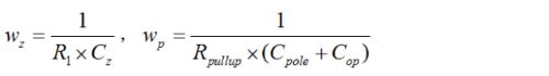
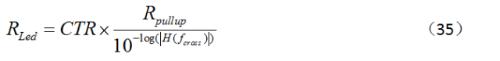
CTR is current transfer ratio of optocoupler, Rpullup is pull-up resistor on secondary side of optocoupler (corresponds to NCP1015, Rpullup = 18 kΩ), Cop is parasitic capacitance of optocoupler related to size of Rpullup. Figure 13 (from Sharp PC817 datasheet) is frequency response of optocoupler. It can be seen that when RL (i.e. Rpullup) is 18 kΩ, it will result in a pole of about 2 kHz, so size of Rpullup will directly affect bandwidth of converter.
The k-factor (k-factor method) was introduced by Dean Venable in 1980s and is a method for determining parameters of a compensation network.
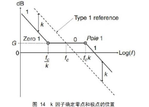
As shown in figure 14, place pole wp of type II compensation network k times fcross and place zero point wz at 1/k fcross. The compensation network in Figure 12 has three parameters to be calculated: RLed, Cz and Cpole and these parameters will be calculated using coefficient k:
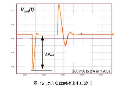
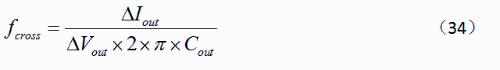
-------Determine compensated loop bandwidth fcross: By limiting overshoot (or undershoot) of output voltage △Vout during dynamic loading (△Iout), loop bandwidth is determined by following formula: < /p>
-------Explore power level transfer characteristics and determine midband gain of the compensation network:
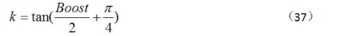
------- Determine Dean Venable factor k: select compensated phase margin PM (typically 55°~80°) and get power level phase shift at fcross by formula 32 (can be calculated from Mathcad) PS, phase Boost that needs to be improved in the compensation network:

Then k is determined by following formula:
-------The compensation network pole (wp) is placed k times fcross, and Cpole can be calculated using following formula:
-------The zero point of compensation network (wz) is placed 1/k times fcross, and Cz can be calculated using following formula:
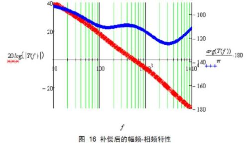
Part 3Checking Simulation
Computer simulation can not only replace many cumbersome manual system analyzes, reduce labor intensity, avoid large errors caused by analytical methods in approximate processing, but also complement each other with physical debugging to minimize design costs. Shorten development cycle.
This example uses classic UC3843 current mode controller (similar to NCP1015 control principle) to create a flyback converter. In this case, parameters of transformer and loop compensation take calculated parameters given in above example.
Simulation Test Conditions: Low Voltage Input (90 VAC Dual Full Load)
1. Scheme
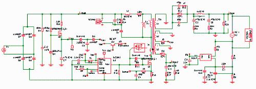
Figure 17. Schematic diagram of simulation
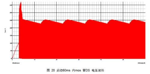
2. Transient Time Domain Analysis
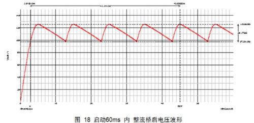
It can be seen from Figure 18 that lowest voltage at lowest Cbulk is 97.3V, which is roughly theoretical value of 98V.
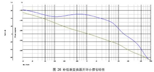
3. AC Frequency Domain Analysis
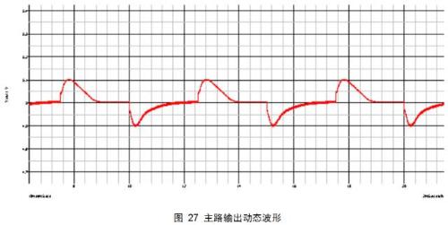
4. Dynamic load curve test
Test conditions: low input voltage, full load, main circuit output current 0.1-1A-0.1A, interval 2.5ms, output voltage test waveform.
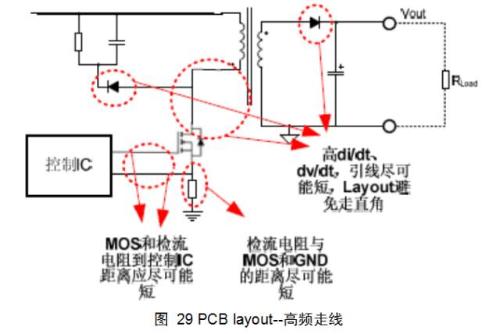
Part 4PCB Design Guide
1. PCB layout. The area surrounded by high current loop should be as small as possible and the wiring should be wide.
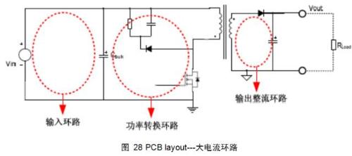
2. PCB layout - high frequency wiring (di/dt, dv/dt)
a. Secondary rectifier, snubber diode, MOS tube and transformer contacts, wires should be as short as possible at these high frequencies, and layout should avoid right angles;
b. MOS tube excitation signal, current detection resistor current detection signal, shorter distance to control IC, better;
c. The distance between sense resistor and MOSFET and ground should be as short as possible.
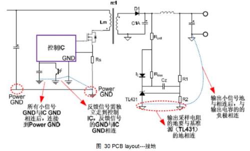
3. PCB Layout - Ground
Basic grounding rules:
a. After all weak signal GNDs are connected to GND of control IC, they are connected to Power GND (that is, strong signal GND);
b. The feedback signal must be fed back to IC independently, and GND of feedback signal is connected to GND of IC.
Secondary Grounding Rules:
a. After output weak signal ground is connected, it is connected to negative pole of output capacitor;
b. The ground of output sampling resistor must be connected to ground of reference signal source (TL431).
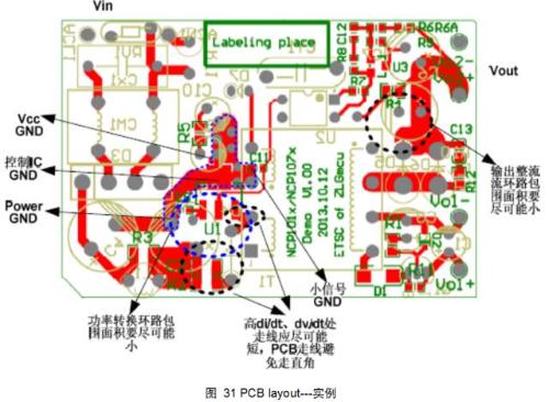
Part 5PCB layout - example
Part 6Overview
This document details flyback converter design steps and issues to consider when designing a printed circuit board, and uses software simulation to validate design's rationale. At same time, appendix shows transfer functions of peak current reverse mode power stage in CCM mode and DCM mode, respectively.
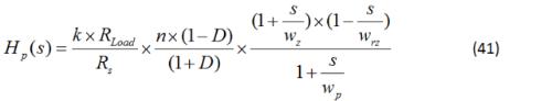
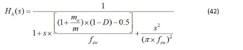
Appendix: Peak current mode Power stage, weak signal
For flyback in CCM mode, transfer from control to output:
The internal peak current mode current loop is essentially a data acquisition system. The power stage transmission consists of two parts connected in series, Hp(s) and Hh(s), where
Hh(s) is second order sampling unit formed by the current loop current sampling (proposed by Ray Ridley):
Where:
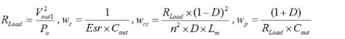
In above formula, PO is apparent output power, k is damping factor from error amplifier output to current comparator input, Vout1 is output voltage of main feedback loop, Rs is damping factor. current detection resistor on primary side, and D is duty cycle of converter. The duty cycle, n is turn ratio of primary coil NP and main circuit feedback coil Ns1, m is rising slope of primary current, ma is compensation slope of slope compensation, Esr is equivalent series resistance of output capacitor, and Cout is sum of output capacitors.
Note. In flyback converter in CCM mode, transfer function from control to output can be seen from formula 40, there is a zero point in right half plane, which causes phase to decay by 90 ° as amplitude increases, this Zero point is not what we need, and design must ensure that passband frequency does not exceed 1/3 of frequency of zero point of right half-plane; from formula 41, if there is no slope compensation (ma=0), when duty cycle exceeds 50%, oscillations of current loop appear as the excitation of large and small waves, that is, subharmonic oscillations. Therefore, tilt compensation must be added when designing a flyback CCM.
For DCM flyback mode, transfer from control to output:
Where:
Vout1 is DC voltage at output of main circuit, k is attenuation ratio from output of error amplifier to input of current comparator, m is upslope of primary current, ma is slope of slope compensation, and Idspeak is primary peak current under given conditions .
Related
- Notes on whole switching power supply design process!
- Switching Power Supply PCB Design Skills
- Finally, it becomes clear that process of obtaining switching losses of a MOSFET in a switching power supply
- 6500 words about switching power supply design, haberdashery, collect first, then study!
- The best switching circuit design process for power supplies is a must for engineers!
- Various losses inside switching power supply
- Do not underestimate "form of high-frequency magnetic core" in switching power supply, what effect does it have on transformer?
- Analysis of damping RC circuit of a switching power supply "haberdashery"
- Power Knowledge - Flyback Transformer Design Process
- Detailed analysis of the "various protection schemes" of a switching power supply
Hot Posts
 How to distinguish induction from leakage, we will teach you three tricks! Ordinary people can also learn super practical
- What is drowning in gold? Why Shen Jin?
- This is a metaphor for EMI/EMS/EMC that can be understood at a glance.
- How many types of pads have you seen in PCB design?
- Summary of Common PCB Repair Techniques
- What is three anti-paint? How to use it correctly?
- Knowing these rules, you will not get confused looking at circuit diagram.
- How to make anti-interference PCB design?
- Can diodes do this?