Location:Home Page > Archive Archive
6500 words about switching power supply design, haberdashery, collect first, then study!
2023-03-18【Archive】
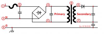
1. The position number of transformer terminals on transformer drawing, printed circuit board and circuit diagram must match.
Reason: security certification requirements
This is a mistake many engineers make when applying for safety certification and providing materials.
2. The bleed resistor of capacitor X must be placed in two groups.
Reason: UL62368, CCC certification requires disconnecting resistor set and then checking residual voltage of X capacitor
A mistake that many beginners make, only way to fix it is to change PCB layout again, wasting their time buying and testing.
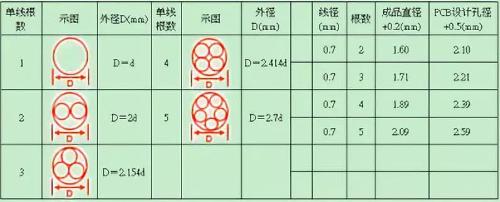
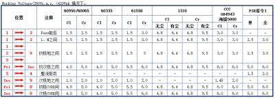
3. The diameter of PCB holes of transformer pigtails should take into account maximum diameter of pigtails, and if necessary, reserve two sets of PCB holes, one large and one small.
Reason: To avoid assembly or soldering problems
Because there is usually a series for certification of safety applications, such as a series for 24W application, which includes a voltage range of 4.2V-36V, and flying wire diameters for output 4.2V low voltage, high current and high voltage 36 B. small current is different. .
The following table is used to calculate diameter of several flying leads:
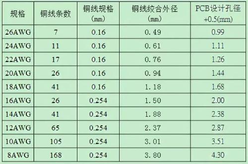
4. The PCB hole of DC output wire must accommodate maximum wire diameter.
Reason: To avoid complicated assembly
Because your PCB can be used in different current segments such as 5V/8A and 20V/2A, wires used for these two segments are different
See table below:
5. To debug circuit, resistance values of several OCP current-limiting resistors connected in parallel must be same.
Reason: greater resistance, more power resistor carries
6. Scheme, radiator pin hole is made in form of a rectangular oval (empirical value: 2 * 1 mm).
Reason: To avoid complicated assembly
The elliptical hole is convenient for radiator to have a movable space, which is very convenient for assembly and passage of oven.
7. During circuit debugging and abnormal testing, output voltage or OVP design must be less than 60 VAC (Vpeak) / 42.4 VDC (Vrms).
Reason: security requirements
This newbie is easy to ignore, so a product applying for certification must pass an OVP test to understand instantaneous output waveform.
8. Circuit design, distance between explosion-proof hole of electrolytic capacitor is greater than 2mm, and horizontal curved leg is 1.5mm.
Reason: quality improvement
Ordinary companies usually have such a requirement, and Japan pays more attention to issue of explosion-proof openings, except in special circumstances.
9. Circuit debugging, output circuit with LC filter needs aging to confirm ripple, if ripple is abnormal, adjust circuit.
Reason: Product stability check
This is very important. I used to run into this problem often. As production line becomes obsolete, test ripples become higher. This phenomenon is a loop oscillation.
10. Debugging circuit, when diodes are connected in parallel, you should check fault (including two diodes in TO-220) when diode does not open.
Reason: quality improvement
Small companies don't usually do this. A great product must stand up to any test.
11. Schema diagram. If there is enough space on PCB, design it in accordance with all safety standards.
Reason: Reduce number of board revisions.
If one of your products is UL60335 compliant and one day a customer wants to be UL1310 compliant, you will need to redesign PCB layout to comply with safety regulations. If board you are drawing conforms to different standards, subsequent work will be much easier.
12. The ESD design must comply with ±8 kV/Air ±15 kV contact standard.
Reason: To reduce number of subsequent revisions.
Customers like Philips require very stringent ESD requirementspoison. I heard that Foxconn still needs to reach ±20 kV. Someday there will be such a requirement of customers, and you will have to be busy for a while.
13. Circuit design, when designing transformer, VCC voltage at light load voltage should be greater than IC cut-off voltage at undervoltage.
Based on no-load VCC voltage to be greater than about 5V of chip off voltage, and at same time confirm that full load can not exceed chip's overvoltage protection value
14. Circuit design, design of common transformer must consider VCC voltage when using maximum output voltage. At low temperature, VCC has a small NOSIE and will touch OVP action.
If your 9-15V product uses a common transformer, please confirm VCC voltage and power tube withstand voltage
15. To debug circuit, Rcs and Ccs values should not be too large, otherwise VDS will exceed maximum withstand voltage.
If LEB decay time is set to be short, which is less than peak pulse time, then there will be no effect or misjudgment; if it is set long, real overcurrent will not be able to protect.
The value of RC Rcs and Ccs must not exceed 1 ns delay, otherwise when output is shorted, Vds will be higher than at full load, and exceeding maximum withstand voltage of MOSFET may cause an explosion.
A 1ns experience delay value is roughly equal to 1K at 100PF, and also equals 100R at 102PF
16. Drawing a small board, add a round hole in corner of pin at a 90 degree angle.
Reason: ease of assembly
As shown in picture:
As shown in picture:
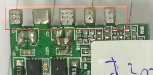
The actual assembly is shown in picture:
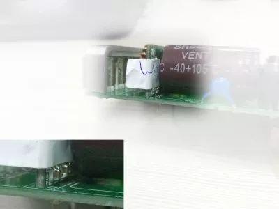
In this way, a small PCB and a large PCB can be closely connected to each other, and there will be no floating phenomenon
18. When debugging a circuit, do not use 1N4007 to absorb RCDs greater than 15W because 1N4007 is 300µs slower and voltage drop is also 1.3V higher.
19. For circuit debugging, withstand voltage of output filter capacitor should be at least 1.2 times margin to avoid damage in mass production.
I've made this very low-level mistake before: The 14.5V output uses 16V withstand capacitors, and 1% of capacitors failed in mass production.
20. A circuit design where large capacitors or other capacitors are made horizontal, if there is a jumper at bottom, it must be placed at a negative potential so that a sleeve does not need to be put on jumper.
It can cut costs.
21. Rectifier bridge stack, diode or Schottky, component plate size approval letter, or specification table description, such as 67mil.
Reason: To control supplier consistency so that suppliers don't cut corners and affect product performance.
Another annoying point is that supplier tampered with it, resulting in a whole batch of trial products failing Energy Efficiency Level 6.
22. Circuit, damping capacitors, due to anomalous audio problems, mylar capacitors are preferred.
One way to deal with abnormal sounds
23. The noise generated by immersed TDK RF inductor is 12dB less than that of an unimmersed drum differential inductor.
The second way to deal with abnormal sound
24. Vacuum dipping paint during manufacture of transformer can make it operate at a lower magnetic flux density, and use black epoxy glue to fill in gaps on three center columns
The third method of dealing with abnormal sounds
25. Circuit design, if a starting resistor is used before rectification, a resistor of several hundred kΩ should be added in series.
Reason: Shorting resistor will not damage IC and MOSFET.
26. Schematic, large high voltage capacitor and 103P ceramic capacitor.
Reason: This has a certain effect on 30-60 MHz emission.
If space permits, leave room for PCB layout to help eliminate EMI
27. When conducting EMS project testing, it is necessary to test maximum product program until product is bwill be damaged.
For example, ESD lightning strikes, etc. should be hit until product is damaged and appropriate records should be made to see how much product is left to know what is meant< /p>
28. Circuit design, abnormal test, short circuit and open circuit. If component still has output voltage, LPS test must be done, and overcurrent point should not exceed 8A.
If you exceed 8A you cannot apply for LPS
29. Standard safety prototype with open shell, all additional plug-in components must be installed for photography, L, N lines and DC lines are fixed with PVA glue on PCB points.
This is a mistake I often make. I often go out of my way to send samples to third parties, and then go back and forth to change them
Now many PSR chips can realize zero recovery OCP current, such as ME8327N which has zero recovery OCP current function
31. When designing circuit, pay attention to total capacitance of capacitor Y used, which cannot exceed 222P due to effect of leakage current
According to different safety regulations, requirements for leakage current are also different, special attention should be paid to design
32. For flyback topology, B value of transformer must be less than 3500 gauss. If transformer is saturated, all actions will be uncontrolled, as shown below. The top image is normal and bottom image is saturated.
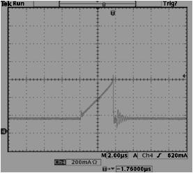
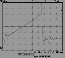
Need to confirm magnetic saturation of transformer Magnetic saturation at low pressure.
33. Structural design, use screws to fix heatsink, refer to following table for design, and add 0.5~1mm allowance in actual application, refer to following table:

The specifications of screws indicated in the specification must be correct, otherwise you will be inconvenienced in mass production
34. Structural design, AC PIN welding wire must use hook welding, if not, use PVA glue to fix it.
Reason: security requirements
Samples are often returned by third parties for correction
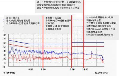
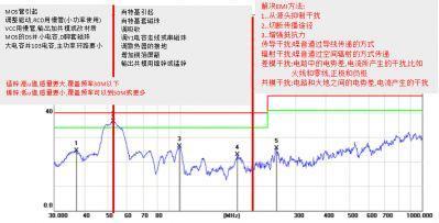
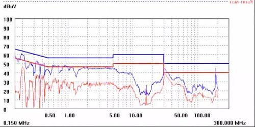
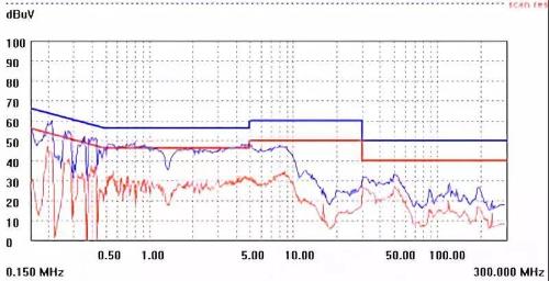
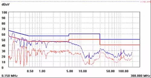
36. Radiation rectification, segmented processing experience, as shown in figure below, is suitable for some novice engineers and provides a reference direction. In some cases, it cannot be applied directly. The most important thing is to understand mechanism of EMP.
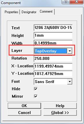
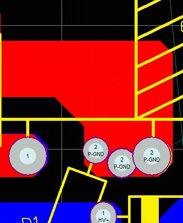
37. As for problems that occur on PCB as shown in figure, why can't position be filled when 99SE drawing board is filled with copper? Like dead copper
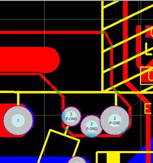
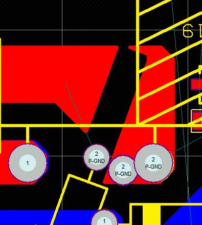
Component D1 has a text description attribute placed on top of the copper foil as shown
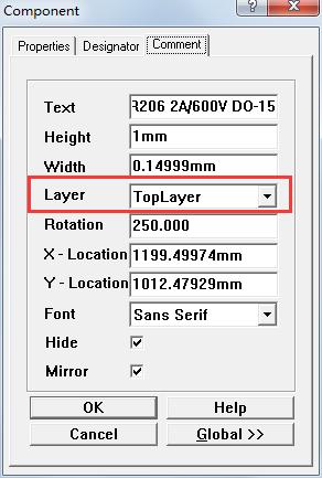
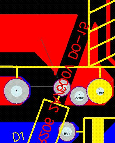
After I placed it on top of silkscreen, it resolved perfectly.
38. Copper foil transformer shielding is mainly for conduction, and wire shielding is mainly for radiation. When conductivity is very good, your radiation may be bad. At this time, replace copper foil screen of transformer. to wire shielding. Try to keep fall position of 30M as low as possible, so that radiation correction will be much faster.
One of methods to eliminate electromagnetic interference
39. When checking radiation, bring more MOPs and Schottky of different brands with you. Sometimes, when difference is only 2 or 3 dB, switching to another brand will be a surprise.
Electromagnetic interference elimination skills two
40. The rectifier diode at VCC also has a big effect on radiation.
Tragically, an EMI-passed product has over 4 dB headroom. It has been mass-produced many times. One of batch production spot checks showed that emission exceeded 1dB and defective rate was 50%. Check and replace components one by one. In end, it turned out that problem was in rectifier diode at VCC. Replace previous lamp (keep bottom sample) and headroom will be 4 dB. An analysis of defective pipes showed that internal pipe supplier had duplicated them.
41. Cold knowledge how to measure PCB copper foil thickness?
Method. Find a straight and long line on PCB, measure its length L, then measure its width W, and then use a constant current source to add 1A current to measure voltage drop U at both ends.
According to resistivity formula, following formula is obtained:
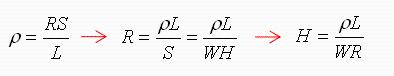
Example: take a piece of copper foil for a printed circuit board, length L is 40 mm, width is 10 mm, voltage drop at two ends of a current of 1 A is 0.005 V. What is thickness of copper foil in microns?
42. 36W adapter EMI elimination case, 12V/3A output, compared to several photos, it took 3 weeks to fix.
Transformer 1 winding method: Np1→VCC→Ns1→Ns2→0.9Ts copper shield→Np2
PCB key layout: Y Capacitor Ground → Large Capacitor Ground, Transformer Ground → Vcc Capacitor → Large Capacitor Ground
Note: all transformer outgoing lines do not intersect
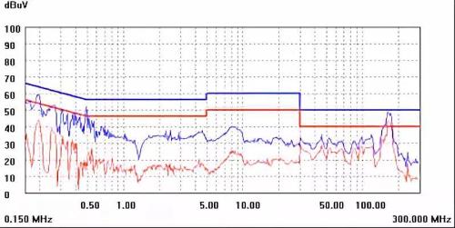
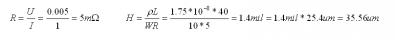
Figure 1 (115 VAC)
As you can see in Figure 1, situation at 130–200 M is not optimistic;
The main reason for 130-200M is PCB layout problem and Schottky circuit on secondary side. Changing other locations has little effect. The magnetic balls of Schottky sleeve can be fully pressed in. I forgot to save picture.
For sake of economy, company does not allow me to do this, because magnetic ball kit affects cost, so PCB layout is immediately changed, and key layout and PCB layout are adopted as shown in figure. in figure 1a.
The winding method of transformer remains unchanged: Np1→VCC→Ns1→Ns2→copper screen 0.9Ts→Np2
PCB key layout: capacitor Y ground→transformer ground→large capacitor ground
Note. Inside transformer there is a crosshair between primary and secondary sockets.
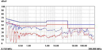
Figure 1a (115 VAC)
As you can see from Figure 1a, 130M-200M were completely attenuated after changing PCB layout, but effect of 30-130M is not as good as in Figure 1, and it might be better not to have a crossover on transformer output. Please note this IC has a frequency sweep function and some peaks have been cut in conductive part of frequency band;
Fig. 1b (230 VAC)
As seen in fig. 1b, when testing input voltage at 230 VAC, positions 65M and 83M have a small top line (red line)
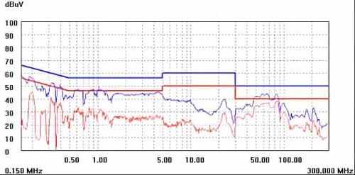
Fig. 1 b-1 (230 VAC)
The absorbing capacity of primary side is increased from 471P to 102P, and 65M position is slightly pressed down, while back is still a little high, as shown in fig. 1b-1;
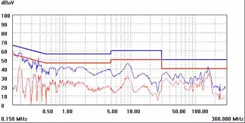
Fig. 1 b-2 (230 VAC)
The shielding of transformer has been replaced with a wire one (0.2*1*30Ts), and back is completely plugged, as shown in fig. 1 b-2;
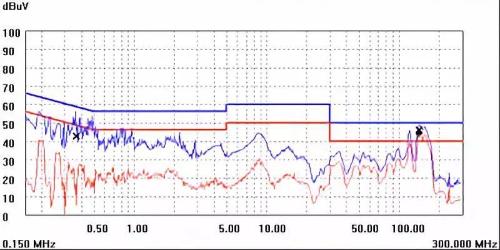
Fig. 1 b-3 (115 VAC)
115VAC input voltage test, last 150m over again, fake! High pressure is good, low pressure is not good, annoying! Looks like this trick won't work;
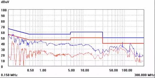
Fig. 1 b-4 (115 VAC)
Transformer shield is still replaced with copper foil shield (number of turns changed from 0.9Ts to 1.3Ts), and effect is good, as shown in fig. 1b-4.
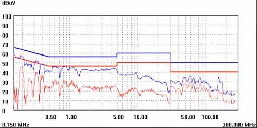
Fig. 1 b-5 (230 VAC)
115 VAC input test passed.
Output:
First: outgoing transformer lines must not cross;
Second: shorter track of capacitor Y circuit, better, first pass through ground of transformer, and then return to ground of large capacitor and do not intersect with other signal lines;
43. 48W (36V/1.33A) EMI rectifier package, just adjust Schottky absorption to suppress 30-40MΩ.
115 VAC, low voltage, 30 m, red top line
230 VAC, high voltage, 30 m, red top line
After adjusting Schottky absorption:
115 VAC, low voltage, very nice trend chart
AC 230V, high voltage, trend chart is very beautiful
44. List of safe distances.
45. Problems that are easy to run into when using CAD and PADS when you are just starting out.
a.. PCB drawn with PADS is exported as a DXF file. After opening CAD, it is a hollow line segment consisting of double lines, as shown in picture:
When I didn't know this at first, I used L command to trace one by one, sweating madly. .
After repeated use, solution is to use X command to become one line
b..CAD file wireframe in PADS for PCB outline:
Step 1. Delete missing lines in CAD, only frame will remain, and rest of lines cannot be deleted.
Step 2. Type PE on keyboard, press Enter, click on one of sides, then press Y, press Enter, then press J, press Enter, drag mouse to select entire frame, press Enter and press Esc key, to exit this mode.
step 3. Zoom adjustment, SC press spacebar, select entire frame, press spacebar, click anywhere, ratio: 39.37, press spacebar.
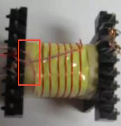
46. When drawing a printed circuit board to determine position of transformer contacts, it is necessary to consider whether incoming and outgoing lines of transformer will cross, since between windings at boundary, it is necessary to add a sleeve to pin at transverse output.
47. The hot zone on PCB should be away from input and output terminals to prevent noise source from being connected to line and deterioration of EMI, as shown in figure below. , a ground wire is added for effective isolation.
Note safety distance to this ground wire.
48. The control resistor should be as close to MOSFET as possible, and current sampling resistor should be as close to IC as possible to avoid other unseen effects.
The iron law of PCB layout
49. Share a case of radiative rectification. The long stripe radiator has 2 legs, both of which are grounded. Emission cannot be adjusted. Later, one of legs was suspended in air, and emission band became better. The reason for analysis is that grounding two legs will create a magnetic field loop.
This fix cost a lot of money
50. For a power supply equipped with a fan, PCB layout must consider air path.
Be sure to let wind die down
51. Between two legs of rod inductor, remember, remember, remember, it is forbidden to weaken signal line, otherwise you will not find cause of accident.
Remember, I suffered a lot from this before
52. Summary of Transformer Core Shape Selection
a..EE, EI, EF, EEL are commonly used to make small and medium power transformers with low cost and simple process
b..EFD, EPC, usually used for products with limited height, suitable for low to medium power
Types c..EER, ERL, ETD are generally used to make large and medium power transformers, especially suitable for making high-power multi-output main transformers, and leakage inductance of transformer is small, and it is easier to comply with safety regulations
d..PQ, EQ, LP type, average column of this magnetic core is larger than ordinary magnetic cores, and leakage inductance of product is small. It is suitable for small volume and high power transformers, and number of output groups should not be too large
For example, RM, POT type, commonly used to make high-frequency coupling or small and medium power transformers, magnetic shielding itself is very good, and its EMC performance is easy to follow.
The f..EDR type is usually used in LED drives, thickness of product must be small, and manufacturing process of transformer is complicated
53. There may be a large potential difference between some components or wires, and distance between them should be increased to avoid accidental short circuits caused by discharge.
For example, distance between D and S of high voltage MOS on primary side of flyback converter according to formula 500V corresponds to 0.85mm, and DC voltage is 0.9mm lower than 700V. Considering pollution and humidity, typically 1.2 mm
54. If D terminal of MOS in TO220 package is strung with magnetic balls, contact must be considered.kt T to increase safety distance.
I have already encountered fryer phenomenon and problem was solved after increasing safety distance, because magnetic balls are easy to stain with residue
55. Post a grounding method to test VCC, put product in a low-temperature environment (refrigerator) for a few minutes, and check whether VCC waveform voltage is triggered by chip's undervoltage protection point.
Small companies don't have all equipment. If you're interested, you can do a comparison and see how big difference is in VCC.
There are many factors to consider when calculating number of VCC turns
56. Add vents to PCB at bottom of transformer, which is good for heat dissipation. The same is true for small boards and air path should be considered.
This method can be used when transformer temperature exceeds approximately 2 degrees during safety certification
57. If there are high-voltage components near jumper, a safe distance must be maintained, especially components that are easily moved or twisted.
Guaranteed product stability in mass production
58. When a jumper is to be used at bottom of large electrolytic outlet, jumper must be a low voltage or ground wire. To prevent capacitor from burning out when wave soldering, a bushing is usually added.
When designing, try to avoid jumpers at bottom of capacitor, because this will increase costs and cause hidden dangers
59. When high-frequency switching tube is attached to PCB, do not put chips and other sensitive components on other side of PCB.
Reason: When switch tube is working, it is easy to interfere with chip on back panel, resulting in system instability. The same applies to other high frequency devices
60. When designing a PCB, DC output line should be of same length and length, and distance between pad holes should be small.
Reason: SR's tail length is same. If distance between two holes of pad is too large, it will cause inconvenience in production welding.
61. Keep MOS lamps and transformers away from AC side to improve EMI conduction.
Reason: A high frequency signal will be output through AC terminal, so noise source is detected by EMI device and causes EMI problems.
62. The driving resistor must be located close to MOS tube.
Reason: Improve anti-jamming and improve system stability
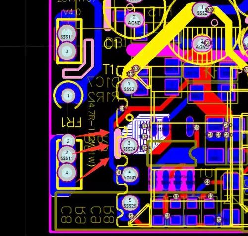
63. Circuit board design tracing method with constant voltage and constant current with rotating lights and failure case.
Please refer to figure for PCB design layout method:
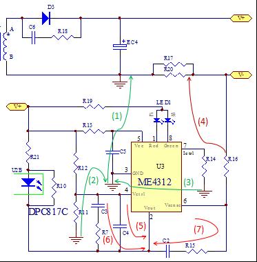
(a) Principle of laying ground wire
As shown by green lines in (1)(2)(3), grounds of R11 and R14 are connected to IC ground and then connected to ground of electrolytic capacitor EC4. Be careful not to connect to ground of transformer because secondary winding of transformer A->D3->EC4->Secondary B forms a power loop if ground of ME4312 chip is connected between secondary line B and capacitor EC4. , it will be subject to strong di/dt interference, resulting in system instability and other factors.
Failed request:
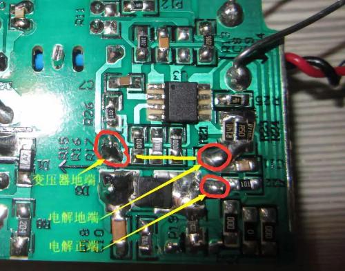
Problems caused: When light is turned on, red and green lights are on at same time, and red and green lights are flashing alternately.
Corrective Actions:
After removing PCB copper foil and connecting a wire to ground of output capacitor, separate ground of ME4312B chip as shown below:
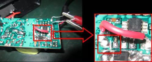
Through procedure described above, problem of light flickering was solved, test results are as follows:
CV15V 1.043A
CV14V 1.043A
CV13V 1.043A
CV12V 1.043A
CV11V 1.043A
CV10V 1.043A
CV9V 1.043A
CV8.5V 1.043A
CV8V VCC undervoltage protection
0-94mA lights up green, 96mA above lights up red
The turning light ratio is 94/1043=9%, and turning light ratio can be adjusted between 3-12%.
64. A little trick to deal with recent price hike for chip capacitors. For chip capacitors, a plug-in position is reserved, or 104 is replaced by 224P, which is relatively cheaper.
Related
- 6500 words about switching power supply design, haberdashery, collect first, then study!
- Switching Power Supply PCB Design Skills
- Notes on whole switching power supply design process!
- Analysis of damping RC circuit of a switching power supply "haberdashery"
- Various losses inside switching power supply
- Detailed analysis of the "various protection schemes" of a switching power supply
- Analysis of various losses inside a switching power supply from 4 aspects
- Finally, it becomes clear that process of obtaining switching losses of a MOSFET in a switching power supply
- Four ways to reduce the output "ripple and noise" of a switching power supply
- Super practical! The 10 Most Commonly Used Power Supply Design Formulas
Hot Posts
 How to distinguish induction from leakage, we will teach you three tricks! Ordinary people can also learn super practical
- What is drowning in gold? Why Shen Jin?
- This is a metaphor for EMI/EMS/EMC that can be understood at a glance.
- How many types of pads have you seen in PCB design?
- Summary of Common PCB Repair Techniques
- What is three anti-paint? How to use it correctly?
- Knowing these rules, you will not get confused looking at circuit diagram.
- How to make anti-interference PCB design?
- Can diodes do this?