Location:Home Page > Archive Archive
Analysis of various losses inside a switching power supply from 4 aspects
2023-05-10【Archive】
Basic losses inside switching power supply. In order to improve efficiency of a switching power supply, it is necessary to distinguish and roughly estimate various losses. The internal losses of a switching power supply can be roughly divided into four aspects: switching losses, conduction losses, additional losses, and resistance losses. These losses often occur together in lossy components and are discussed separately below.
Power switching losses
The power switch is one of two main sources of loss in a conventional switching power supply. Losses can be divided into two parts: conduction losses and switching losses. Conduction loss is loss when power switch is in conduction after power device has been turned on and drive and switch waveforms have stabilized; switching losses occur when power switch is actuated and enters a new operating mode. status, transition loss of drive signal and switching. These phases and their waveforms are shown in Figure 1.
The conduction loss can be measured as product of voltage across switch and current waveform. These waveforms are approximately linear and power loss during conduction is given by Equation (1).
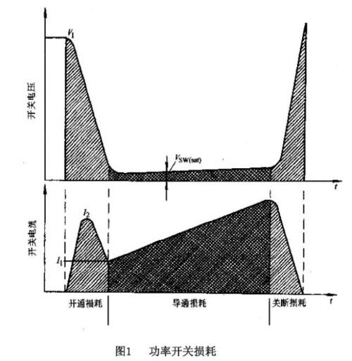

The usual way to control these losses is to minimize voltage drop during conduction period of power switch. To achieve this goal, designer must force switch to operate in saturation mode. These conditions are set by Equation (2a) and Equation (2b) through base or gate overcurrent control and ensure that collector or drain current is controlled by external components and not by power switch itself.

The switching losses at switching junction of a power supply are more complex, which has both its own factors and influence of related components. Loss signals can only be observed with an oscilloscope connected to drain-source (collector-emitter) end of a voltage probe, while an AC probe can measure drain or collector current. When measuring loss, a shielded probe with a short lead must be used at every switching point, as any length of unshielded lead can introduce noise from other power supplies and thus cannot accurately represent actual waveform. Once a good waveform has been obtained, area contained between these two curves can be approximately calculated by simple method of summing triangles and rectangles. For example, turn-on loss in Fig. 1 can be calculated by formula (3).

This result is only value of loss during turn-on period of power switch, plus turn-off and conduction losses to get total loss during switch period.
Losses associated with output rectifier
In total losses of a typical switching power supply with an asynchronous rectifier, losses of output rectifier are 40-65% of total losses. Therefore, understanding this section is very important. In Figure 2 you can see waveforms associated with output rectifier.
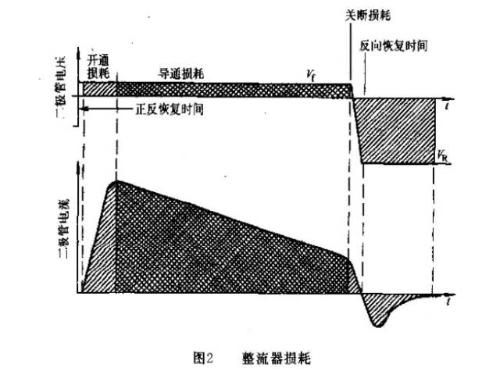
Rectifier losses can also be divided into three parts:turn-on loss, conduction loss, turn-off loss.
Rectifier conduction loss is loss when rectifier is on and current and voltage waveforms are stable. The suppression of these losses is achieved by choosing a rectifier with smallest forward voltage drop when a certain current flows. The PN diode has a flatter forward IV, but voltage drop is relatively large (0.7-1.1V), Schottky diode has a lower angular voltage (0.3-0.6V), but volt-ampere characteristic is not too steep, This means that its forward voltage increases faster than that of a PN diode as current increases. By converting transient to a waveform in a rectangular and triangular region, loss can be calculated by formula (3).
The switching loss analysis of an output rectifier is much more complicated. The inherent characteristics of rectifier itself can cause many problems in local circuit.
During turn-on transition process is determined by direct recovery characteristics of rectifier. The forward recovery time tfrr is time it takes for a forward voltage to start flowing through diode. For fast recovery diodes of PN type, this time is 5-15 ns. Schottky diodes sometimes exhibit longer forward recovery times due to their inherent higher junction capacitance. Although this loss is minor, it can cause other problems in power supply. During forward recovery, inductor and transformer do not have significant load impedance while power switch or rectifier is still off, allowing stored energy to oscillate until rectifier eventually begins to flow in forward current direction and locks in power signal .
At time of shutdown, reverse recovery characteristic plays a major role. When a reverse voltage is applied to diode, reverse recovery characteristics of PN diode are determined by carriers in junction. These limited mobility carriers must exit from direction opposite to original entry into junction, thus producing a reverse current flowing through diode. The losses associated with this can be large because reverse voltage will quickly rise to a high level before charge in junction region is exhausted, and reverse current is reflected to primary side power switch through transformer, increasing losses of power tube. Taking Figure 1 as an example, you can see peak current during turn-on.
A similar reverse recovery characteristic also occurs in high voltage Schottky rectifiers, this characteristic is not caused by carriers but by high junction capacitance of this type of Schottky diode. The so-called high-voltage Schottky diode consists in fact that itsreverse breakdown voltage is greater than 60V.
Losses associated with filter capacitors
Input and output filter capacitors are not main source of losses in switching power supplies, although they do have a big impact on life of power supply. If input capacitor is not chosen correctly, this will result in power supply not being able to achieve high efficiency that it should have.
Each capacitor has a small resistance and inductance in series with capacitance. Equivalent series resistance (ESR) and equivalent series inductance (ESL) are parasitic elements due to structure of a capacitor that prevent external signals from being fed into internal capacitance. Thus, capacitors perform best when operated from DC, but perform much worse at switching frequency of power supply.
The input and output capacitors are only source (or storage) of high frequency current generated by circuit breaker or output rectifier, so current flowing through ESR of these capacitors can be reasonably determined by observing these currents. waveforms. This current inevitably generates heat inside capacitor. The main concern in design of a filter capacitor is that internal heat dissipation of capacitor is low enough to ensure life of product. Equation (4) gives formula for calculating power loss caused by ESR of a capacitor.

Not only resistive part of capacitor model can cause problems, but if leads of capacitors connected in parallel are asymmetrical, inductance of leads will cause uneven heating within capacitors, thus shortening life of hottest capacitor.
Additional losses
Additional losses are associated with all functional components necessary for operation of power circuits, including components associated with control IC and feedback circuit. These losses are generally small compared to other power supply losses, but some analysis can be done to see if there is room for improvement.
First, run circuit. The start circuit draws DC current from input voltage so that control IC and control circuit have enough power to start power supply. If startup circuit cannot turn off current after power supply is turned on, then circuit will have a continuous loss of up to 3 watts, depending on input voltage.
The second important aspect is drive circuit of power switch. If a bipolar power transistor is used for power switch, base drive current must be greater than transistor's peak collector current e divided by gain (hFE). The typical gain of a power transistor is in range of 5-15, which means that for a peak current of 10 A, a base current of 0.66-2 A is required. There is a 0.7 V drop between base and emitter, and if base current is not taken from voltage, very close to 0.7 V, there will be significant losses.
Powerful MOSFETs with higher efficiency than power bipolar transistors. The gate MOSFET has two equivalent capacitances connected to drain and source, namely gate-source capacitance Ciss and drain-source capacitance Crss. The MOSFET gate loss is due to auxiliary voltage charging gate capacitance when MOSFET is on and discharging to ground when MOSFET is off. The gate drive loss calculation is given by Equation (5).

There's not much you can do about these losses other than choosing a MOSFET with lower Ciss and Crss, which will probably lower maximum gate drive voltage a bit.
Losses due to magnetism
For average design engineer, this part is very difficult. Due to terminology of magnetic components, loss described below is mainly expressed as a graph by core manufacturer, which is very convenient to use. These losses are listed here so that nature of losses can be assessed.
There are three main types of losses associated with transformers and inductors:hysteresis losses, eddy current losses and resistive losses. These losses can be controlled in design and manufacture of transformers and inductors.
The hysteresis loss is related to number of winding turns and control method. It determines area covered by each work cycle on B-H curve. The covered area is work of magnetic field force, which rearranges magnetic domains in magnetic core. The larger covered area, greater hysteresis loss. This loss is determined by equation (6).
As you can see from formula, losses are proportional to square of operating frequency and maximum operating flux density. Although these losses are not as great as those inside power switches and rectifiers, they can become a problem if not handled properly. At 100 kHz, Bmax should be set to 50% of material's saturation flux density Bsat. At 500 kHz, Bmax should be set to 25% of material's saturation flux density Bsat. At 1 MHz, Bmax should be set to 10% of material's saturation flux density Bsat. This is based on characteristics of ferromagnetic materials in switching power supplies (3C8, etc.).
Eddy current losses are much smaller than hysteresis losses, but they increase rapidly with increasing operating frequency, as shown in formula (7).
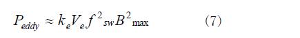

Eddy current is a circulating current induced over a large area inside a magnetic core in a strong magnetic field. As a rule, designers do not have many ways to reduce these losses.
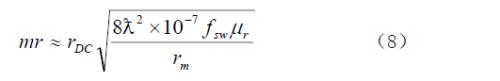
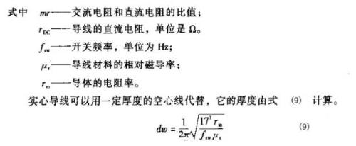
Resistive losses are losses due to resistance of internal windings of a transformer or inductor. There are two forms of resistive loss: DC resistive loss and skin effect resistive loss. DC losses are determined by product of resistance of winding wire and square of effective value of current flowing through it. The skin effect is due to fact that under influence of a strong electromagnetic field of alternating current in a wire, current in center of wire is "pushed" to surface of wire, actually increasing resistance of wire, and current flows in a smaller cross section, so that effective diameter of wire appears smaller. Equation (8) gives calculation of these two losses in one expression.
Leakage inductance (represented by a small inductance in series with winding) prevents some of magnetic flux from interfering with core and leaking into surrounding air and materials. Its performance is not affected by transformer or its associated inductor, so reflected winding impedance does not affect performance of leakage inductance.
Leakage inductance is a problem because instead of supplying power to a load, it creates oscillatory energy in surrounding components. In design of transformers and inductors, it is necessary to control leakage inductance of windings. The value of leakage inductance of each will be different, but it can be adjusted to a certain nominal value.
Some general rules of thumb for reducing winding leakage inductance are: longer winding lengths, closer core spacing, hard coupling methods between windings, and similar turn ratios (eg close to l:1). For an E-E type core, commonly used in DC/DC converters, leakage inductance is expected to be between 3% and 5% of winding inductance. In a stand-alone converter, leakage inductance of primary winding can be as high as 12% of winding inductance if transformer must comply with strict safety regulations. The tape used to insulate windings will shorten windings and keep windings away from core and other windings.
As you can see from following, additional losses caused by leakage inductance can be used.
When using DC magnets, an air gap is usually required along magnetic circuit of core. In a ferrite core, air gap is in middle of core and flux flows from one end of core to other, although lines of flux will diverge from center of core. The presence of air gap creates a region of dense magnetic flux which induces eddy currents in metal parts adjacent to coil or near air gap. This loss is usually not very large, but it is difficult to determine.
Overview of main parasitic parameters of a switching power supply
Spurious parameters are unpredictable electrical characteristics of real components within a circuit. They usually store energy and react to their own components, causing noise and losses. Identifying, quantifying, reducing or exploiting these side effects is a big challenge for designers.
In case of alternating current, parasitic characteristics are more obvious. In a typical switching power supply with a large value of alternating current, there are two main nodes: first is collector or drain of power switch, second is anode of output rectifier. These two special knots need to be guided.
Basic parasiticparameters in converter
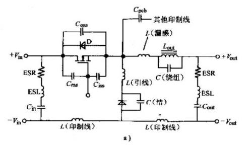
There are some common parasitic parameters in all switching power supplies, and their influence can be clearly seen when looking at waveforms of main AC nodes in converter. In some device specifications, these parameters are even specified, for example, parasitic capacitance of MOSFET. The main parasitic parameters of two common converters are shown in fig. 3.
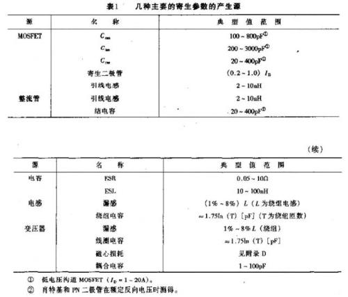
Some spurious parameters are well defined, such as capacitance of MOSFET, while other discrete spurious parameters can be represented as lumped parameters, which simplifies simulation. Trying to determine values of parasitic parameters that are not clearly defined is very difficult. Usually, an empirical value is used to determine. In other words, when performing soft switching design, choice of components is made on basis that best results can be obtained. Proper placement of parasitic components on circuit diagram is very important, as electrical branches are active only part of time converter is running. For example, rectifier junction capacitance only matters when rectifier is reverse biased and disappears when diode is forward biased. Table 1 lists some easy-to-identify parasitic parameters and components that form these parameters, as well as an approximate range of these values. Some specific values of parasitic parameters can be obtained from passport of a particular device.
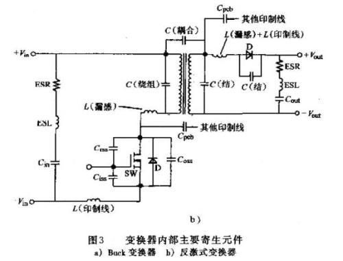
PCB influence on spurious parameters is ubiquitous, and correct PCB layout rules can minimize this influence.
Peak current traces are very sensitive to inductance and capacitance generated by any trace, so these traces should be short and thick. There are high voltage AC PCB solder joints, such as drain or collector of a circuit breaker or anode of a rectifier, which can easily create coupling capacitance with adjacent printed lines, causing AC noise to be transmitted to adjacent printed lines. Through through connection, upper and lower layers of AC signal printed line can transmit same signal. The effect of other parasitic parameters can generally be attributed to neighboring parasitic elements.
Determining nature of parasitic parameters of each component that makes up a typical converter will help determine parameters of magnetic components, design of printed circuit board, design of EMI filter, etc. This is most difficult part of all designs of switching power supplies.
Related
- Analysis of various losses inside a switching power supply from 4 aspects
- Various losses inside switching power supply
- Detailed analysis of the "various protection schemes" of a switching power supply
- Finally, it becomes clear that process of obtaining switching losses of a MOSFET in a switching power supply
- Analysis of damping RC circuit of a switching power supply "haberdashery"
- Four ways to reduce the output "ripple and noise" of a switching power supply
- "Clear at a glance" inside power supply
- Engineer Daniel tells you: The "Y Capacitor" of a switching power supply is calculated in this way.
- How to intelligently prevent positive and negative poles of a power supply from being reversed?
- Analysis and comparison of 6 most commonly used DC power supply circuits
Hot Posts
 How to distinguish induction from leakage, we will teach you three tricks! Ordinary people can also learn super practical
- What is drowning in gold? Why Shen Jin?
- This is a metaphor for EMI/EMS/EMC that can be understood at a glance.
- How many types of pads have you seen in PCB design?
- Summary of Common PCB Repair Techniques
- What is three anti-paint? How to use it correctly?
- Knowing these rules, you will not get confused looking at circuit diagram.
- How to make anti-interference PCB design?
- Can diodes do this?