Location:Home Page > Archive Archive
What is a delay scheme? Explanation of 6 Kinds of Delay Circuit Principles
2023-04-23【Archive】
As we all know, when it comes to latency, a lot of people think about using software components like timers and like. Today we will talk about how to implement timing in hardware, although it is not so accurate, but in some cases it can still be used. Today we will introduce you to principles of operation of 6 delay circuits.
1. Accurate circuit diagram with long delay
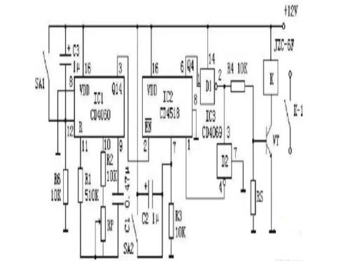
The circuit consists of a CD4060 as a time base time base circuit. The time base pulse generated by circuit is divided by an internal frequency divider to output a time base signal. By frequency division of peripheral frequency division circuit, required timing control time is achieved.
When turned on, time base generator oscillates and outputs a time base signal after frequency division. IC2 as a frequency divider starts counting frequency division. When count reaches 10, Q4 outputs a high level, and high level is turned low by inversion of D1, so that VT turns off and relay is released when power is turned off, cutting off working power of controlled circuit.
At same time, low level output of D1 is inverted by D2 to a high level, and then added to CP terminal of IC2, so that a high level output remains at output terminal.
After energizing circuit to reset IC1 and IC2, all four output terminals of IC2 are low. The low level at output of Q4 is changed to a high level through inversion of D1, and VT is turned on through R4, and relay is energized and absorbed. This operating state is a power-on state and a time state.
2. RC delay circuit
The RC delay circuit is shown in figure. The delay time of circuit can be adjusted by R or C size. However, due to simple delay circuit, there are disadvantages of short delay time and poor accuracy. For cases requiring long delay times and requiring accuracy, it is better to use a time relay.
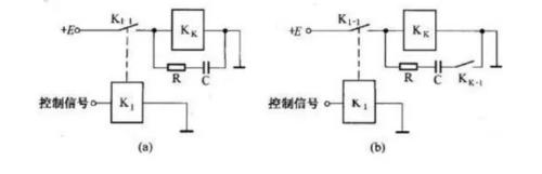
In automatic control, sometimes a delay relay circuit is often used to force controlled object to run for a given period of time or to issue next work command at appropriate time. The figure shows several relay delay circuits.
The circuit shown in Figure (a) is a slow absorption circuit. As circuit turns on and off, RC charge and discharge are used to implement pull in and release delay. This circuit is mainly used for a short delay when closing suction. Sometimes, according to control needs of relay, it only needs to be slowly released, but not allowed to slowly retract. At this time, circuit shown in figure (b) can be used.
When power is turned on for first time, since KK-l contact is normally open, RC delay circuit will not delay pull-in time, and K relay will act as a relay. After retracting it, contact Kk-1 closes, so that relay kk can be uncoupled slowly. Just calculate time delay generated by RC delay circuit, for example R=470K, C=0.15uF, time constant by directly using R*C on line.
3. A simple circuit with a long delay, consisting of 555
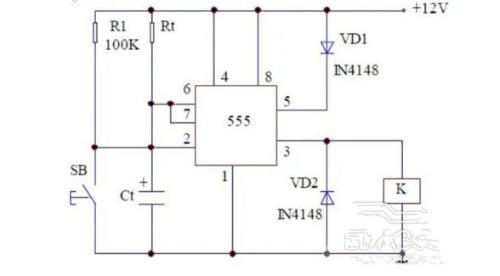
When SB button is pressed, 12V power supply charges capacitor Ct through resistor Rt, continuously raising potential on pin 6. When potential on pin 6 rises to potential on pin 5, reset time of circuit is reset. ends.
Because VD1 diode is connected to 5-pin string to raise potential of 5-pin string, it has a longer time interval than a normal connection (hanging or grounding through a small capacitor).
4. Long delay circuit consisting of two 555 sweep circuits
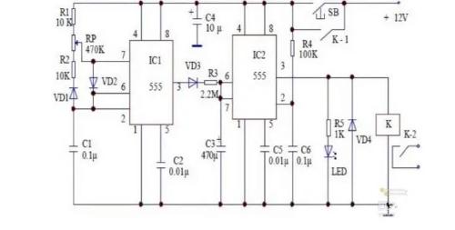
The timing base circuit IC1 555 is included as a self-excited, variable-duty multivibrator. When SB button is pressed, a constant voltage of 12V is added to circuit. Since voltage of capacitor C6 cannot change abruptly, pin 2 of IC2 circuit is low, IC2 circuit is in setting state, and pin 3 outputs a high level, and relay when K is energized, contacts K-1 and K-2 are closed, and contact K-1 is closed to form a self-latching state, and contact K-2 is connected to electrical equipment to perform function of controlling on and off of electrical equipment.
At same time, time base circuit of IC1 555 starts to oscillate, so pin 3 outputs high and low levels alternately. When a high level appears at pin 3, capacitor C3 is charged through diode VD3 and resistor R3.
When pin 3 is low, VD3 turns off and C3 is not charged, so C3 only charges when pin 3 is high, so C3 takes longer to charge.
When C3 rises to 2/3VDD, IC2 555 sweep resets, pin 3 goes low, relay K loses power, pins K-1 and K-2 open and reset. to prepare for the next time.
5. Single-op-amp monostable delay
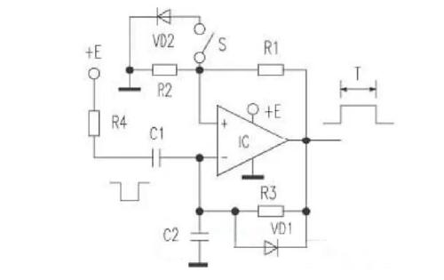
In normal state, output signal of microcircuit remains at a low level, this state is stable. When a negative pulse is applied to inverting terminal through C1, potential of inverting terminal is lower than that of non-inverting terminal, and output terminal switches from low to high. This state is unstable.
A high level is added to non-inverting terminal of IC after dividing by R1 and R2, so that potential of non-inverting terminal is higher than potential of inverting terminal to maintain a high level. level output. At same time, high level is charged by R3 and C2. When voltage across C2 is charged to make potential of inverting terminal higher than potential of non-inverting terminal, output terminal switches to low again. .
At this time, potential of non-inverting terminal is near zero, and voltage at C2 is quickly discharged to output terminal through VD1, so that circuit accelerates to return to its original state.
After circuit stabilizes, potential of inverting terminal is still higher than potential of non-inverting terminal, so that output can be kept low.
The delay time T of this circuit depends not only on R3 and C2, but also depends on voltage division ratio of R1 and R2.
Therefore, it is very convenient to adjust delay time. You can adjust C2 and R3 for coarse delay adjustment and R2 for fine adjustment (if voltage division ratio is 1/2 to 2/3, delay accuracy is higher).
However, state of circuit at power up is random, so there are two ways to give circuit a unique output state after power up:
First, add R4 to circuit. Thus, when power is on, since voltage at C1 cannot suddenly change, supply voltage is added to inverting terminal through R4 and C1, and output can be set to low;
Second is to connect diode VD2 and switch S between non-inverting terminal and ground (as shown by dotted line).
If output is high at power-up, although this state is unstable as mentioned above, it will take time T before output is low. In practice, this is often necessary to reset circuit immediately on power-up.
For this reason, when you turn on power, you can turn on S first. If output is high, then C2 can be charged to 0.7V to reset circuit, which greatly reduces time to reset circuit at power on. Disconnect S after reset and circuit can work normally.
6. Transistor delay circuit
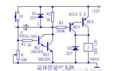
The delay part consists of BG1, BG2 and capacitor C, forming a Miller integrated circuit. Before power is turned on, voltage at terminal C is zero. After power on, BG3 and BG4 are on and relay J is closed. At same time, capacitor C is charging, and charging current forms a loop through resistors R2, C, and R. The potential of point a rises, causing potential of point b to drop, and drop in potential of point b limits potential of point a to rise.
As a result of mutual compensation of potentials of points a and b, increase in potential of point a is very small, and charging current is almost constant.
When potential at point b rises to about 10V, BG3 and BG4 are close to tripping, relay J opens and delay process ends. Press AN button once, capacitor C will quickly discharge through D1, relay J will close, and next delay process will begin.
Delay circuits are often used, and RC circuits are relatively simple. Of course, different delays can be achieved by changing parameters of each circuit component.
Related
- What is a delay scheme? Explanation of 6 Kinds of Delay Circuit Principles
- How did BUCK scheme come about? Application: 3 kinds of evolutionary chains
- What does inside of a multilayer PCB look like? Three-dimensional general analysis of design process of high-quality printed circuit boards
- Principal analysis of BUCK / BOOST circuit, a summary is also in place
- Analysis of power circuit of a classic single-chip microcomputer
- Analysis of damping RC circuit of a switching power supply "haberdashery"
- What is purpose of connecting a polar capacitor and a non-polar capacitor in parallel?
- A detailed explanation of role of pull-up resistors on triodes and MOS lamps.
- In circuit design, what are differences between six types of grounds?
- A detailed explanation of three commonly used LED drive power schemes.
Hot Posts
 How to distinguish induction from leakage, we will teach you three tricks! Ordinary people can also learn super practical
- What is drowning in gold? Why Shen Jin?
- This is a metaphor for EMI/EMS/EMC that can be understood at a glance.
- How many types of pads have you seen in PCB design?
- Summary of Common PCB Repair Techniques
- What is three anti-paint? How to use it correctly?
- Knowing these rules, you will not get confused looking at circuit diagram.
- How to make anti-interference PCB design?
- Can diodes do this?