Location:Home Page > Archive Archive
"Easy to understand" Miller effect when switching MOS lamps
2023-04-16【Archive】
Basic principles of Miller's platform formation
The gate driving process of a MOSFET can be simply understood as process of charging and discharging a drive source to input capacitance of MOSFET (basically gate-to-source capacitance Cgs); when Cgs reaches threshold voltage, MOSFET enters open state; When MOSFET is turned on, Vds starts to fall and Id starts to rise, at which time MOSFET enters saturation; but due to Miller effect, Vgs will not rise for a certain period of time, at which time time Id has reached its maximum, and Vds continues to fall until Miller capacitor is fully charged and Vgs rises to value of control voltage. At this time, MOSFET enters resistance zone. At this time, Vds drops completely and switch-on ends.
Because Miller capacitor prevents Vgs from rising, it also prevents Vds from falling, which increases loss time. (As Vgs increases, the on-resistance decreases, so Vds decreases)
The Miller effect is notorious in MOS drives. This is Miller effect caused by Miller capacitance of MOS lamp. During turning on of MOS lamp, GS voltage is stable after GS voltage is increased. up to a certain voltage value. , and then voltage of memory begins to rise again until it is fully turned on. Why is there a stable value? Because D pole voltage is greater than G pole voltage before turning on MOS, and electricity stored in MOS parasitic capacitance Cgd must be injected into G pole to neutralize charge when it is turned on, because G pole voltage is greater than D pole voltage after full inclusion of MOS. The Miller effect will seriously increase turn-on losses of MOS. (MOS lamps cannot quickly enter switching state)
This is how so-called totem driver appeared! ! When MOS is selected, smaller Cgd, lower turn-on loss. The Miller effect cannot be completely eliminated.
The Miller platform in a MOSFET is actually a typical indication that a MOSFET is in "boost zone".
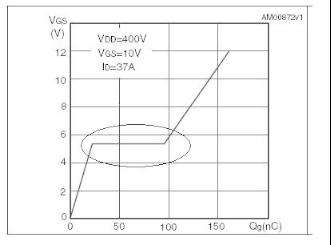
Measure GS voltage with an oscilloscope and you will see that there is a platform or pit in voltage rise process which is Miller platform.
Detailed Miller platform formation process
The Miller effect means that when MOS tube is turned on, a Miller platform will be generated. The principle of operation is following.
Theoretically, Miller effect can be eliminated by adding a sufficiently large capacitance between G-class and S-class in excitation circuit. But at this time, switching time will be very long. It is useful to add a capacity value of 0.1Cess to overall recommended value.
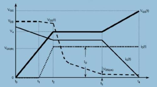
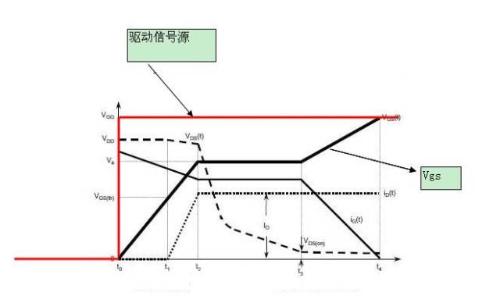
The flat part of thick black line in image below is Miller platform.
This load drop factor graph is at first turning point: Vds begins to conduct. The change in Vds forms a differential through Cgd and internal resistance of excitation source. Since Vds decreases approximately linearly, linear differential remains constant, resulting in a plateau at Vgs.
Miller's platform is called capacity g d mos, which is Crss in description of mos.
This process is for charging Cgd, so Vgs changes very little. When Cgd charges up to Vgs, Vgs starts to keep rising.
When mos is first turned on, Cgd is rapidly discharged through mos and then re-charged by control voltage, dividing control current so that voltage across Cgs slowly rises and a plateau appears.
t0~t1: Vgs from 0 to Vth. Mosfet is defective. Current flows through parasitic diode Df.
t1~t2: Vgs from Vth to Va.
t2~t3: Vds drops, causing current to continue flowing through Cgd. The higher Vdd, more time is required. Ig is control current. It starts falling faster when Vdg is close to zero, Cgd increases until Vdg becomes negative, Cgd increases to a maximum and fall slows down.
t3~t4: MOSFET is fully on, working in resistance region, Vgs continues to rise to Vgg.
In late stage of platform, VGS continues to grow, but IDS changes little because MOS is oversaturated. . . However, judging by picture from poster, this platform still has a certain length.
During this platform period, MOS can be considered to be in an expansion period.
Before previous inflection point: MOS deadline, Cgs charged at this time, Vgs approaching Vth.
At previous tipping point: MOS has officially entered a period of gain.
At next inflection point: MOS officially exits its gain period and begins to enter its saturation period.
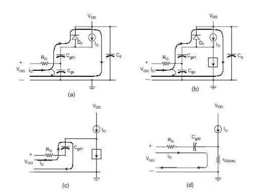
When a voltage V with slope dt is applied across capacitor C (for example, output voltage of a driver), current in capacitor will increase:
I=C×dV/dt (1)
So when MOSFET is energized, it will generate an input current Igate = I1 + I2 as shown in figure below.
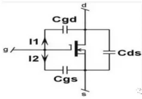
Using formula (1) for right stress node, we can get:
I1=Cgd×d(Vgs-Vds)/dt=Cgd×(dVgs/dt-dVds/dt) (2)
I2=Cgs×d(Vgs/dt) (3)
If a MOSFET is supplied with a gate-to-source voltage, Vgs, its drain-to-source voltage, Vds, will drop (even if drop is non-linear). Therefore, negative gain connecting these two voltages can be defined as:
Av=- Vds/Vgs (4)
Substituting formula (4) into formula (2), we can get:
I1=Cgd×(1+Av)dVgs/dt(5)
During conversion (on or off), total equivalent capacitance Ceq of source gate is:
Igate=I1+I2=(Cgd×(1+Av)+Cgs)×dVgs/dt=Ceq×dVgs/dt (6)
The term (1+Av) in formula is called Miller effect, which describes capacitive feedback between output and input in electronic devices. When gate-drain voltage is close to zero, Miller effect occurs.
The most powerful step in Cds shunting is in expansion zone. Why? Because it is at this stage that Vd changes most dramatically. It is at this stage that platform is formed. You might think that: the gate current of Igate is completely absorbed by Cds, and no current flows on Cgs.
Pay attention to representation in data sheet:
Ciss=Cgs+Cgd
Coss=Cds+Cgd
Crss=Cgd
Related
- "Easy to understand" Miller effect when switching MOS lamps
- What skills should I pay attention to when designing a triode amplifier circuit? (Easy to understand)
- Easy to understand! Explain PID
- A detailed explanation of role of pull-up resistors on triodes and MOS lamps.
- Do you understand MOS driver in motor controller?
- MOS tube drive circuit, how to make MOS tube turn on and off quickly?
- Do not underestimate "form of high-frequency magnetic core" in switching power supply, what effect does it have on transformer?
- Four ways to reduce the output "ripple and noise" of a switching power supply
- Three circuit diagrams to teach you how to understand how a buck RC works
- Welding knowledge and skills that electronics professionals need to understand
Hot Posts
 How to distinguish induction from leakage, we will teach you three tricks! Ordinary people can also learn super practical
- What is drowning in gold? Why Shen Jin?
- This is a metaphor for EMI/EMS/EMC that can be understood at a glance.
- How many types of pads have you seen in PCB design?
- Summary of Common PCB Repair Techniques
- What is three anti-paint? How to use it correctly?
- Knowing these rules, you will not get confused looking at circuit diagram.
- How to make anti-interference PCB design?
- Can diodes do this?