Location:Home Page > Archive Archive
7 things you need to know about high-speed linking and routing
2023-03-18【Archive】
What knowledge and skills should engineers have when designing high-speed circuits? Below is a detailed description of seven technical aspects to answer them one by one.
01 Power Supply Diagram and Wiring
Digital circuits often require intermittent current, so some high-speed devices will surge current.
If power supply trace is very long, it will cause high frequency noise due to presence of inrush current, and this high frequency noise will be introduced into other signals. In high speed circuits, there must be parasitic inductance, parasitic resistance and parasitic capacitance, so high frequency noise will eventually be coupled to other circuits, and presence of parasitic inductance will also lead to maximum surge current that can occur in wiring. can withstand a drop resulting in a partial voltage drop that could destroy circuit.
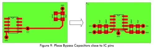
It is therefore especially important to add bypass capacitors before digital devices. The larger capacitance, more power transfer is rate-limited, so a large capacitor and a small capacitor are usually combined to match full frequency range.

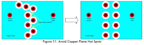
Avoid hotspots: Signal vias will create voids on power layer and bottom layer. Therefore, inappropriate placement of vias can lead to increased current density in certain areas of power supply or ground plane. And these places where current density increases are called hot spots.
Therefore, we must do our best to avoid such a situation when setting up vias to avoid plane splitting, which will eventually lead to EMC problems.
Usually best way to avoid hotspots is to place vias in a gridstyle so that current density is uniform and the planes are not isolated and there is no way back . If it is too long, there will be no EMC problems.
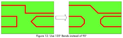
02 How wires are bent
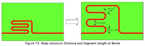
When laying high-speed signal lines, care should be taken to avoid signal line bends. If you need to bend tracks, do not lay tracks at sharp or right angles, but use obtuse corners instead.
When laying high-speed signal lines, we often achieve equal lengths by laying coils. The same coils are actually a kind of bend in wiring. The line width, spacing, and bending method must be reasonably chosen, and spacing must comply with 4W/1.5W rule.
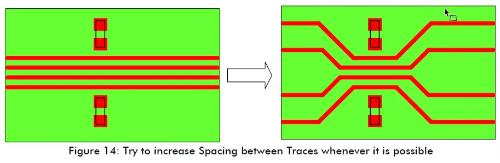
03 Signal proximity
If distance between high speed signal lines is too small, crosstalk may occur. Sometimes, due to layout, frame size, and other reasons, distance between high-speed signal lines we lay exceeds minimum required distance, so we can increase distance between high-speed signal lines as much as possible near bottleneck distance.
In fact, if there is enough space, try increasing distance between two high-speed signal lines.
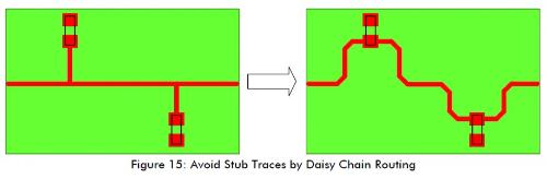
04 wire lengths
The long cable is equivalent to an antenna, mishandling it will cause serious EMC problems.
At same time, stub will also cause reflections and reduce signal integrity. Usually, when a pull-up or pull-up resistor is added to a high-speed signal line, a stub is likely to form, and typically stub wiring can be chrysanthemum.
According to experience, if stub line is longer than 1/10 of wavelength, it can be used as an antenna, and this will become a problem at present.
05 Impedance discontinuity
The impedance value of a trace usually depends on width of trace and distance between trace and reference plane. The wider track, lower its impedance. And some interface terminals are also device pads, and this principle is also applicable.
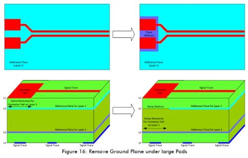
When pad of interface terminal is connected to high-speed signal line, if pad at that time is especially large and high-speed signal line is especially narrow, impedance of large pad is small, and narrow trace must have a large impedance, in which case there will be an impedance break , and breaking impedance will cause signal to be reflected.
In general, to solve this problem, a forbidden copper shell is placed under interface terminal or large pad of device, and pad reference plane is placed on another layer to increase impedance and make impedance continuous.
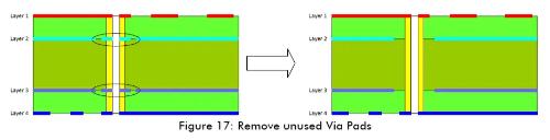
Transitions are another source of impedance inhomogeneities. To minimize this effect, unwanted copper on inner layers and junctions must be removed.
In fact, such an operation can be eliminated by using CAD tools during design or by contacting and communicating with PCB manufacturers to eliminate unnecessary copper jacket and ensure impedance continuity.
06 Differential signal
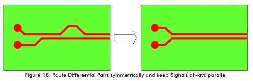
For high-speed differential signal lines, we must provide same width and same distance to get a certain value of differential impedance. Therefore, try to ensure symmetry when laying differential signal lines.
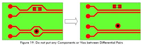
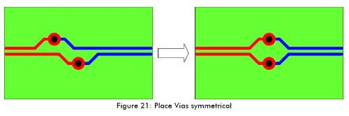
Do not place vias or components on a differential line pair. If vias or devices are placed on a differential line pair, EMC problems will occur and an impedance break will occur.
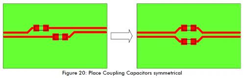
Sometimes some high-speed differential signal lines need to be connected in series with coupling capacitors. The coupling capacitor should also be arranged symmetrically, and packing of coupling capacitor should not be too large. It is recommended to use 0402, 0603 is also acceptable. It is better not to use capacitors higher than 0805 or parallel capacitors.
Vias typically create huge impedance discontinuities, so for pairs of high-speed differential signal lines, keep number of vias to a minimum, and if you are going to use vias, arrange them symmetrically.
07 Equal length
In some high-speed signaling interfaces, such as buses, arrival time and delay error between signal lines must be taken into account. For example, arrival times of all data signal lines in a group of high-speed parallel buses must be within a certain time delay error to ensure their settling and hold times are consistent. To fulfill this requirement, we must consider equal lengths.
A high-speed differential signal line must provide a strict time delay between two signal lines, otherwise communication may be broken. Therefore, to satisfy this requirement, equal lengths can be realized with serpentine lines, thereby satisfying time delay requirement.
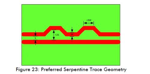
A serpentine line should generally be placed at source of loss of length, not at far end. Only at source can signals at positive and negative ends of differential line be transmitted synchronously most of time.
Bends in paths are one source of length loss. To bend track, equal length must be close to bend (<=15 mm)
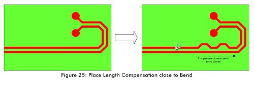
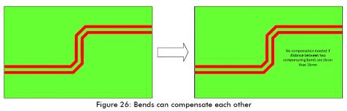
If there are two curved traces and distance between them is <15mm, loss in length of two traces at this time cancels each other out, so there is no need to process equal lengths at this time.
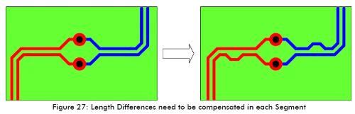
For different sections of high-speed differential signal lines, they must be independent and equal in length. The vias, serial communication capacitors and interface terminals will be divided into two parts by high-speed differential signal lines, so special attention should be paid at this time.
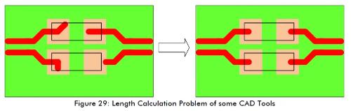
Must be equal in length. Because many EDA programs only pay attention to whether length of entire course is exceeded during DRC.
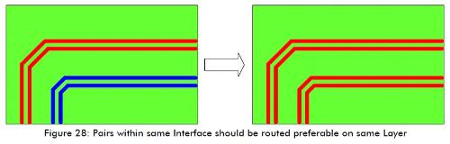
For interfaces such as LVDS display devices, there will be multiple pairs of differential pairs at same time, and timing requirements between differential pairs are generally very stringent, and time delay requirements are particularly low. Therefore our requirements for such differential signals are usually within compensation in same plane. Because signal transmission speed of different layers is different.
When any EDA software calculates length of a trace, trace inside pad will also be included in length. If length compensation is performed at this time, final actual result will be lost. So pay special attention to this time when using some EDA software.
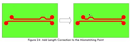
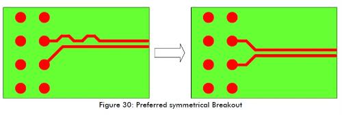
At any time, if possible, you should choose symmetrical outgoing lines to avoid need for final serpentine wiring for equal lengths.
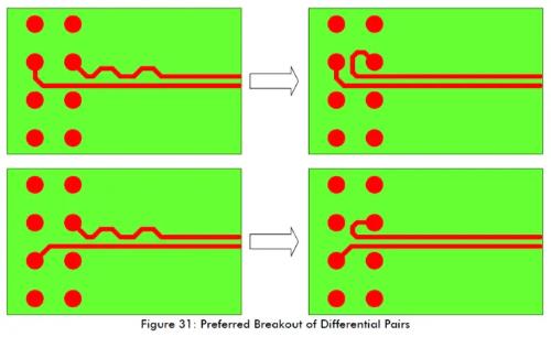
If space permits, try adding a small loop at source of short differential line to compensate instead of compensating through serpentine line.
Related
- 7 things you need to know about high-speed linking and routing
- What you need to know about semiconductor chips
- About resistors, this is what you need to know
- Do you know everything about communication, decoupling and capacitance?
- What do you know about fuse classification?
- Do you know all this little knowledge about inverters?
- "English abbreviations" that equipment engineers need to know
- A Few Design Tips PCB Engineers Need to Know
- step-down capacitor pay attention to these six points, do not need to worry about circuit analysis
- In PCB industry, we all need to know these 5 important common sense rules.
Hot Posts
 How to distinguish induction from leakage, we will teach you three tricks! Ordinary people can also learn super practical
- What is drowning in gold? Why Shen Jin?
- This is a metaphor for EMI/EMS/EMC that can be understood at a glance.
- How many types of pads have you seen in PCB design?
- Summary of Common PCB Repair Techniques
- What is three anti-paint? How to use it correctly?
- Knowing these rules, you will not get confused looking at circuit diagram.
- How to make anti-interference PCB design?
- Can diodes do this?