Location:Home Page > Archive Archive
What you need to know about semiconductor chips
2023-03-25【Archive】
Size reduction has physical limitations
However, production process cannot be reduced indefinitely. When we reduce size of transistor to about 20 nanometers, we will run into problems in quantum physics that will cause leakage in transistor and negate benefits obtained by reducing L . The concept of FinFET (Tri-Gate) is introduced as an improvement method, as shown in upper right figure. In a previous explanation, Intel knew that implementation of this technology could reduce leakage caused by physical phenomena.
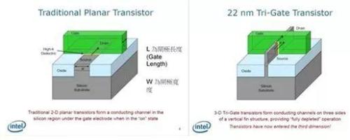
More importantly, this technique can increase area of contact between end of gate and bottom layer. In traditional method (upper left image), contact surface has only one plane, but after introduction of FinFET (Tri-Gate) technology, contact surface will become three-dimensional, and contact area can be easily increased so that same contact can be maintained. The area makes end of Source- The drain is smaller, which helps a lot in reducing size.
Finally, this is why some people say that large manufacturers will face serious problems when moving to 10 nm process technology. The main reason is that size of an atom is about 0.1 nm. In case of 10 nm, a line length less than 100 atoms is very difficult to manufacture, and as long as there is a defect in one atom, such as precipitation of atoms or impurities during production, unknown phenomena will occur that will affect yield of product.
If you're comfortable, do a little experiment. Use 100 small beads to form a 10x10 square on table and cut out a piece of paper to cover beads, then use a small brush to brush away beads next to it, and finally make a 10x5 rectangle. In this way, we can find out what difficulties large factories face and how difficult it is to achieve this goal.
As Samsung and TSMC will complete mass production of 14nm and 16nm FinFET in near future, both want to compete for Apple's next generation iPhone chip foundry, we will see a very exciting business competition, and at same time, you will get more energy-saving, thinner and lighter mobile phones thanks to benefits of Moore's law.
As mentioned above, chip manufacturing process is similar to building a Lego house. First, wafer is used as a base, and after chip manufacturing process is laid down layer by layer, required IC chips can be produced. However, without blueprints, it is useless to have a strong production capacity, so role of architects is very important. But who is an IC design architect? The following is an introduction to IC design.
In IC manufacturing process, ICs are mainly planned and developed by professional IC design companies such as MediaTek, Qualcomm, Intel and other well-known manufacturers. They all design their own IC chips and provide chips with different features and performance downstream supplier choice. Because ICs are developed in every factory, IC design is highly dependent on skills of engineers, and quality of engineers affects value of enterprise. However, when engineers design an integrated circuit, what are steps? The design process can be simply divided as follows.
The first step in design is setting goals
The most important stage of designintegrated circuits is development of specifications. This step is similar to designing a building: first decide how many rooms and bathrooms you want, what building codes to follow, and design after all features are determined so you don't have to spend extra time on subsequent revisions. When designing an IC, it is also necessary to go through similar steps to make sure that there are no errors in designed chip.
The first step in formulating specifications is to determine purpose and performance of IC, and to determine general direction. The next step is to check which protocols must be followed. For example, wireless network card chip must comply with IEEE 802.11 specifications and others. Otherwise, chip will not be compatible with products on market, making it impossible to connect with other devices. Finally, set implementation method of this IC, assign different functions to different modules, and set communication method between different modules to complete formulation of specification.
After specifications are developed, next step is to develop chip parts. This step is similar to initial drawing of building plan and drawing general outline to make later drawing easier. In IC chips, circuits are described using Hardware Description Language (HDL). Commonly used HDLs include Verilog, VHDL, etc., and IC menus can be easily expressed with program code. The next step is to check correctness of program function and then change it until it corresponds to desired function.
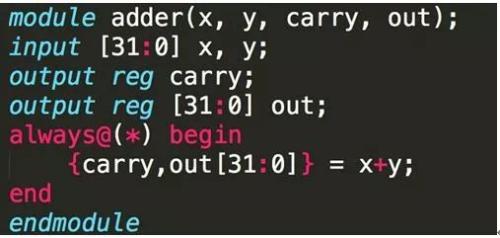
▲ Verilog 32-bit adder example
Computers make it easier
Once you have a complete plan, next step is to create a graphic drawing. In IC design, logic synthesis step is to put error-free HDL code into an electronic design automation tool (EDA tool), let computer convert HDL code into a logic circuit, and create following circuit diagram. After that, it is repeatedly determined whether design diagram of logic element meets specification, and is revised until function becomes correct.

▲ Control block synthesis result
Finally, place synthesized code into another EDA tool for placing and routing circuits (Place And Route). After continuous testing, following circuit diagram will be formed. In picture, you can see different colors such as blue, red, green and yellow, and each individual color is a mask. How to use mask?
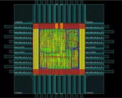
▲ The commonly used computing chip is FFT chip, result of circuit completion and winding
Layer by layer of photomask, stacking chip
Firstly, it is already known that one IC will produce several masks, these masks have different layers, and each layer has its own task. The figure below shows an example of a simple photomask based on CMOS, most basic component in an integrated circuit. combination of NMOS and PMOS to form CMOS. As for metal oxide semiconductor (MOS), this component, which is widely used in chips, is more difficult to explain, and it is more difficult for general reader to understand it, so I will not go into details here.
In figure below, left side is circuit diagram formed after circuit was assembled and wound. We already know that each color represents a photomask. On right is how each mask is distributed. Production must start from bottom layer, follow method mentioned in previous article on IC chip production, and do it layer by layer, and finally desired chip will be produced.
By now, you should have a basic understanding of integrated circuit design. In general, it is clear that design of integrated circuits is a very difficult profession. With maturity of computer software, design of integrated circuits can be accelerated. IC design factories rely heavily on intelligence of engineers. Each step described here has its own specialized knowledge and can be independently formed into several professional courses. For example, writing a hardware description language requires not only familiarity with a programming language, but also needs to understand how logic circuit works, how to convert required algorithm into a program, and how synthesis software converts program into a logic gate.
However, using encapsulation methods described above will require a significant amount of effort. Like modern mobile devices, wearables, etc., quite a few components are required. If each component is packaged separately, it will take up a lot of space when combined. Therefore, there are currently two methods to meet size reduction requirements: SoC (System On Chip) and SiP (System In Packet).
When smartphones first appeared, term "system on a chip" could be found in major financial magazines, but what is a "system on a chip"? Simply put, it is combination of integrated circuits with different functions in one chip. With this method, not only can size be reduced, but also distance between different ICs can be reduced, and computing speed of IC can be improved. Regarding production method, various ICs are brought together during IC design and then made into a photomask using design process presented earlier.
However, SoC has not only advantagescreatures, and SoC development requires significant technical cooperation. When chips are packaged separately, each has an outer package protection, and distance between chip and chip is relatively large, so there will be less mutual interference. But when all chips are put together, nightmare begins. IC development factories must move from simple IC design to understanding and integrating ICs with various functions, which increases workload for engineers. In addition, there will be many situations, for example, high frequency signal of communication chip may affect IC of other functions.
In addition, SoC also needs to obtain intellectual property permission from other manufacturers in order to use components developed by others in SoC. Because to create an SoC, it is necessary to obtain design details of entire IC in order to make a complete photomask, which also increases cost of SoC development. Some people may wonder, why not just design one yourself? Because designing various ICs requires a lot of IC knowledge, only a rich company like Apple has budget to poach best engineers from established companies. - it is more efficient to design a completely new IC through cooperative licensing than to develop it on your own.
Demolition plan, sip appeared
Alternatively, SiP is moving to integrated circuit stage. Unlike SoC, it buys chips from different companies and packages these chips one last time, so that IP authorization step is eliminated, greatly reducing design costs. In addition, since they are separate ICs, degree of mutual interference is greatly reduced.
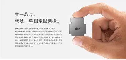
▲ The Apple Watch uses SiP technology to package entire computer architecture into a chip that not only delivers performance you expect, but also reduces size, allowing watch to have more battery space.
Apple Watch is most famous product using SiP technology. Because watch's internal space is too small, it cannot use traditional technology, and SoC development cost is too high, so SiP has become first choice. With SiP technology, not only can size be reduced, but distance between each chip can also be shortened, making it an acceptable compromise solution. The figure below is a block diagram of Apple Watch chip, and you can see that quite a few chips are included in it.
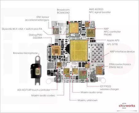
▲ Diagram of internal configuration of S1 chip in SiP case in Apple Watch
Once packaging is complete, it will enter testing phase. At this stage, it is necessary to confirm whether packaged IC is working normally. Once it is correct, it can be sent to an assembly plant to manufacture electronic products we see. So far, semiconductor industry has completed entire production task.
Related
- What you need to know about semiconductor chips
- About resistors, this is what you need to know
- 7 things you need to know about high-speed linking and routing
- What do you know about fuse classification?
- Do you know everything about communication, decoupling and capacitance?
- Do you know all this little knowledge about inverters?
- "English abbreviations" that equipment engineers need to know
- A Few Design Tips PCB Engineers Need to Know
- step-down capacitor pay attention to these six points, do not need to worry about circuit analysis
- In PCB industry, we all need to know these 5 important common sense rules.
Hot Posts
 How to distinguish induction from leakage, we will teach you three tricks! Ordinary people can also learn super practical
- What is drowning in gold? Why Shen Jin?
- This is a metaphor for EMI/EMS/EMC that can be understood at a glance.
- How many types of pads have you seen in PCB design?
- Summary of Common PCB Repair Techniques
- What is three anti-paint? How to use it correctly?
- Knowing these rules, you will not get confused looking at circuit diagram.
- How to make anti-interference PCB design?
- Can diodes do this?