Location:Home Page > Archive Archive
In PCB industry, we all need to know these 5 important common sense rules.
2023-03-23【Archive】
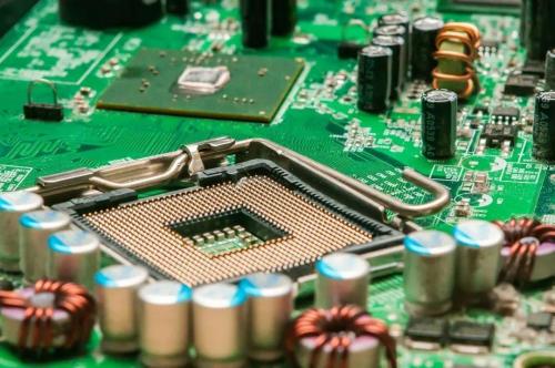
PCB (printed circuit board), Chinese name for a printed circuit board, also known as printed circuit board, which is support housing of electronic components and electrical connection carrier of electronic components.
In electronics industry, if there are electronic components such as integrated circuits, a printed circuit board must be used to ensure uniform electrical interaction between each component.
Next, Circuit Bacteria will share with you five important common senses that we all need to know in PCB industry.
PCB manufacturer chain
The chain of PCB production from top to bottom is as follows: raw materials - middle production - subsequent use of PCBs, as shown in the figure below.
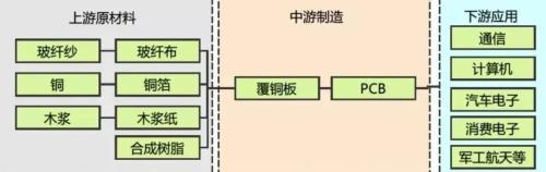
▲PCB production chain diagram
The notable feature of PCB is that it covers a wide range of follow-on applications, covering industries such as computers, communications, consumer electronics, industrial control, medical, military, semiconductors and automobiles, as well as almost all electronic information products.
Among them, computers, communications and consumer electronics are top three applications, accounting for about 70% of cost of PCB manufacturing.
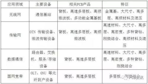
▲Applications and functions of communication PCB
Copper Laminate Classification
Copper Clad Laminate (CCL) is main core material in PCB manufacturing. It is made by impregnating electronic fiberglass cloth or other reinforcing materials with resin, coating one or both sides with copper foil, and hot pressing. Sheet of material.
It accounts for 20% to 40% of PCB production costs and is closely related to PCBs.
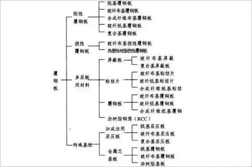
1) Based on mechanical rigidity, copper-clad laminates can be divided into rigid copper-clad laminates (rigid copper-clad laminate) and flexible copper-clad laminates (flexible copper-clad laminate).
2) According to different insulating materials and structures, it can be divided into organic resin copper clad laminates, metal-based copper clad laminates and ceramic-based copper clad laminates.
3) Depending on thickness of copper-plated laminate, it can be divided into thick sheets (thickness range 0.8 ~ 3.2mm (including copper)), thin sheets (thickness range less than 0.78mm (excluding copper) ). ).
4) According to reinforcing material of copper clad laminate, it is divided into glass fiber based copper clad laminate, paper based copper clad laminate and composite based copper clad laminate (CME-1, CME -2).
5) According to degree of fire resistance, boards are divided into fire retardant and non-combustible boards: according to UL standard (UL94, UL746E, etc.), fire resistance grade of CCL is divided into Rigid CCL can be divided into four different types: fire retardant: UL -94V0, UL-94V1, UL-94V2 and UL-94HB.
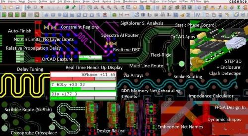
PCB design
PCB design refers to development of hardware design of product. It is an important R&D work connecting hardware PCB circuit design with PCB processing and manufacturing. The project process looks like this:
1) At beginning of project, it is necessary to check whether various materials needed for project are ready: including circuit diagrams, block diagrams, package libraries, signal flow diagrams of complex products, power tree diagrams, key signal descriptions, power supply currents, design request, etc.
2) Input of design information: including import of netlist and block diagram. After importing block diagram, special attention should be paid to size of screw holes and some of positioning holes, forbidden zone of components and wiring, height restriction zone, and position of connector.
3) Layout: place devices on board intelligently based on comprehensive consideration of signal quality, electromagnetic compatibility, thermal design, DFM, DFT, design, safety rules, etc. The main idea of the layout is generally to combine flow signals and power flow in layout in addition to structure constraint.
4) Routing Constraints: Routing constraints are mainly divided into line width, spacing size, equal length, etc. Some rules need to be guided by pre-simulation, such as line length, impedance size, topology, layered structure, etc. .
5) Wiring. Wiring is most important link inPCB design, and there are many things to consider. For example, line impedance, reference plane continuity, EMC, SI/PI, DFM, etc.
6) Inspection + verification after simulation: after completion of connection, verification and verification by senior staff of department, as well as simulation of key signals and power supplies, is required.
7) Processing: After PCB design is approved, light painting file can be output for production.
PCB processing
There are many processes involved in processing and production of printed circuit boards. Whether it's circuit processing, solder mask processing, or silk screen printing, they are all like "printing". This is why PCBs are called "PCBs" or "PCBs". printed circuit board". reason.
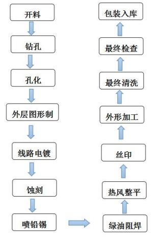
▲Scheme of manufacturing process of a single / double-sided printed circuit board
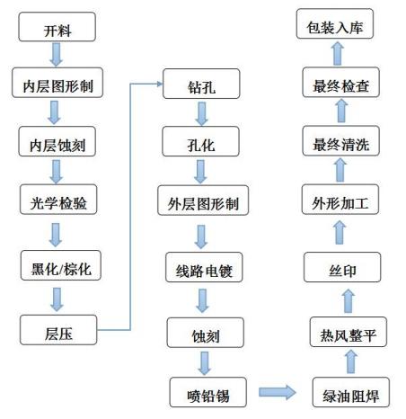
▲Scheme of production process of multilayer printed circuit boards
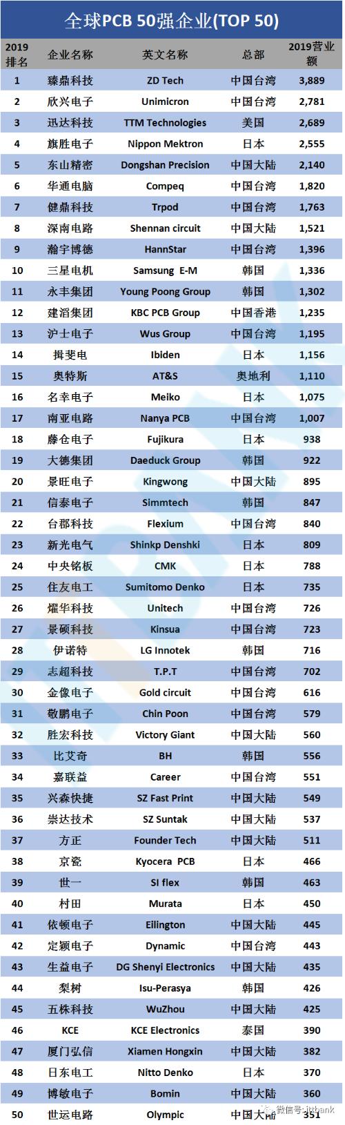
The world's top 50 PCB manufacturers in 2019
There are "strong players" in every industry, just like PCB industry. According to ittbank statistics, list of top 50 PCB companies in world in 2019 is as follows:
Related
- In PCB industry, we all need to know these 5 important common sense rules.
- A Few Design Tips PCB Engineers Need to Know
- PCB puzzle, these few special rules!
- Do you know layout requirements of some special devices in PCB design?
- "English abbreviations" that equipment engineers need to know
- What you need to know about semiconductor chips
- About resistors, this is what you need to know
- Popularizing common sense inductors
- 7 things you need to know about high-speed linking and routing
- Summary of Common PCB Repair Techniques
Hot Posts
 How to distinguish induction from leakage, we will teach you three tricks! Ordinary people can also learn super practical
- What is drowning in gold? Why Shen Jin?
- This is a metaphor for EMI/EMS/EMC that can be understood at a glance.
- How many types of pads have you seen in PCB design?
- Summary of Common PCB Repair Techniques
- What is three anti-paint? How to use it correctly?
- Knowing these rules, you will not get confused looking at circuit diagram.
- How to make anti-interference PCB design?
- Can diodes do this?