Location:Home Page > Archive Archive
Diagram of relationship between PCB layout and EMC
2023-03-18【Archive】
Guide: Talking about complexity of switching power supply, problem of PCB layout is not very difficult, but if you want to route a good PCB board, then switching power supply should be one of difficulties (if design circuit board is not good, it may lead to situation that no matter how to debug parameters, it is not panic). The reason is that there are many factors to consider when laying out a printed circuit board, such as electrical characteristics, processing route, safety requirements, impact of electromagnetic compatibility, etc. Among factors considered, electrical is most basic, but most difficult to understand is electromagnetic compatibility. The bottleneck of many projects is electromagnetic compatibility. This article talks about relationship between PCB layout and EMC in 22 ways.
Firstly, EMI circuit of PCB design can only be done after familiarization with circuit
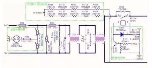
The effect of above circuit on EMC can be imagined, input filter here is voltage sensitive to protect against lightning, resistor R102 to prevent inrush current (interact with relay to reduce losses), key differential mode X capacitors and Y capacitors, which interact with inductance to filter, there are also fuses that affect safety circuit, each device is very important here, and function and role of each device must be carefully studied. When designing a circuit, it is necessary to take into account level of EMC severity in a quiet design, such as specifying several stages of filtering, number and location of Y capacitors. The choice of size and number of varistors is closely related to our EMC requirement. We invite you to discuss a seemingly simple EMI circuit with deep truth in every component.
Second, circuit and EMC: (the most familiar basic flyback topology, see where EMC mechanism is located in circuit)
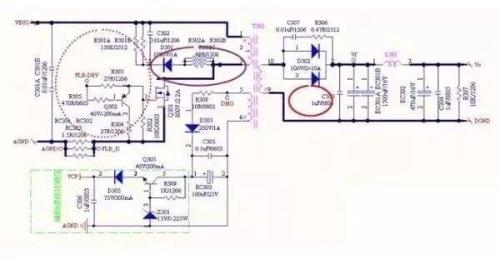
Circle several parts of circuit in figure above: it is very important to influence electromagnetic compatibility (note that green part does not), such as radiation. Everyone knows that radiation of electromagnetic field is spatial, but basic principle is as follows. change in magnetic flux, which includes effective cross section of magnetic field, i.e. corresponding circuit in circuit.
Current can generate a magnetic field, which is a stable magnetic field that cannot be converted into an electric field, but a changing current creates a changing magnetic field, and a changing magnetic field can generate an electric field (actually, this is Maxwell's famous equation. I use popular parlance), a changing electric field can also create a magnetic field. Therefore, we must pay attention to those places with status of switch, which is one of sources of EMC, and this is one of sources of EMC (one of which, of course, is mentioned here, other aspects will be mentioned later), for example, a dotted loop in circuit, this switch tube. And closed loop, not only switching speed can be adjusted when designing circuit, which has an important effect on EMC, but also area of the circuit circuit and wiring! The other two loops are absorption loop and rectification loop. Let's deal with it in advance and talk about it later.
3. Relationship between PCB design and EMC
1. The influence of circuit board circuit on EMC is very important. For example, main power circuit of flyback, if it is too large, radiation will be poor.
2. Filter wiring effect. The filter is used to filter out interference, but if circuit board wiring is poor, filter may lose its proper effect.
3. In structural part, improper design of heatsink grounding will affect grounding of shielding plate, etc.;
4. Sensitive parts are too close to interference source. For example, electromagnetic interference circuit is very close to switch tube, which will inevitably lead to poor EMC, and a clear isolation zone is required.
5. RC absorption circuit wiring.
6. The grounding and routing of Y capacitor and location of Y capacitor are also critical.
Here is a small example:
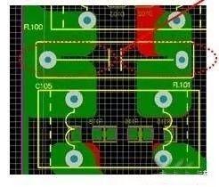
As shown in dotted line in figure above, X capacitor terminal wiring has been removed. You can learn how to make capacitor terminal wiring dangling (use compressed current wiring). In this way, filtering effect of capacitor X can reach best state.
Fourth, PCB design preparation: (only when preparation is sufficient, design can be stable step by step, so as to avoid project tipping over and repeating)
The following aspects are usually considered during design process. All content has nothing to do with other guides and is just a summary of my own experience.
1. Appearance and structural dimensions, including installation holes, duct flow direction, inlet and outlet nozzles, must be consistent with customer's system, and it is also necessary to inform customers about assembly problems, height restrictions, etc.
2. Safety Certification, what type of certification is required for product, where it is necessary to leave a sufficient creepage distance for basic insulation and where to leave a sufficient distance or slot for reinforced insulation.
3. Packing design: Is there any special period, such as preparing to pack non-standard parts.
4. Process route selection: Select single-sided double-sided board or multi-layer board based on comprehensive evaluation of circuit diagram, board size, cost, etc.
5. Other special requirements of customers.
The structure and process is relatively more flexible, and security rules are still a relatively fixed part. What safety and certification standards have been adopted? Of course, there are some safety rules common to many standards, but there are also some special products, such as medical treatment, that are more stringent.
In order not to confuse new engineers, here is a list of some common products. Below are specific layout requirements for IEC60065. You must remember safety rules. When confronted with specific products, they must be addressed purposefully. :
1. Safety regulations require that distance between parts of fuse entry pad be greater than 3.0mm, and actual board layout must be 3.5mm (in other words, 3.5mm creepage path to fuse and 3.0mm creepage path). after).
2. The front and rear rectifier bridge safety regulations require 2.0mm, and layout requires 2.5mm.
3. After straightening, there are generally no safety regulations requirements, but distance between high and low voltage should be set according to actual voltage. It is customary to leave more than 2.0mm for 400V high voltage.
4. The primary and secondary safety regulations require 6.4 mm (electrical clearance) and creepage distance is 7.6mm as best (Note: This is related to actual input voltage and must be calculated by looking up table. The data is for reference only. The actual situation shall prevail).
5. Cold ground and hot ground for primary and secondary use are clearly marked: L, N marks, AC IN input marks, fuse warning marks, etc. must be clearly marked.
If you have any questions about above, you can also discuss them and learn from each other.
Please be reminded that actual safety distance is related to actual input voltage and operating environment. It must be calculated by looking at table. The data is for reference only, and actual situation shall prevail.
5. PCB design safety rules take other factors into account1. Find out what certification your product is manufactured under and what category it belongs to, for example, for medicine, communications, electric power, television, etc. But there is also much in common.
2. In places closely related to PCB layout in safety regulations, one should understand characteristics of insulation, which places are basic insulation, which places are reinforced insulation, and insulation distance of different standards is different. It is best to consult standard and calculate electrical distance and creepage distance.
3. Pay attention to safety components of product, such as relationship between magnetic properties of transformer and primary and secondary sides.
4. Distance between radiator and surrounding area The insulation of radiator depends on floor.
5. Pay special attention to belay distance, where requirements are most stringent. The front and rear fuse distances are same.
6. Relationship between capacitance Y and leakage current and contact current.
In following, we will detail how to keep your distance and comply with safety requirements.
6. PCB Power Schematic
1. First measure size of PCB and number of components so that density is constant, otherwise one part will be dense and other part will be sparse and ugly.
2. Schematic modularity, centering on main components and placing components at same time based on key component priority principle.
3.The devices are arranged vertically or horizontally.One is beautiful and other is convenient for insertion operations.In special cases, tilt can be considered.
4. Wiring must be planned in layout, and it must be placed in most reasonable place to facilitate subsequent wiring.
5. Minimize loop area as much as possible during layout, which will be explained in detail later for four main loops. To achieve above points, of course, it needs to use gibko, and a smarter layout is coming soon.
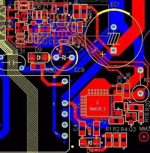
The following is a circuit board that is worth studying in general:
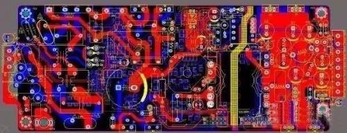
The power density of this image is still relatively high. The LLC control part, auxiliary source part, and BUCK (powerful multi-channel output) circuit driver part are on a small board, so I did not take it outside. Let's look at characteristics of main power layout. Bar:
1. The input and output terminals are fixed and cannot be moved. The board is rectangular. How to choose direction of main power flow? Here layout is arranged from bottom up, from left to right, and heat release depends on shell. 2. The EMI circuit still has a clear flow direction, which is very important, otherwise it is not pretty and not good for EMC.
3. The position of large capacitor maximally takes into account PFC circuit and LLC main power circuit.
4. The current on secondary side is relatively large. This circuit is used to transfer current and dissipate heat from rectifier tube. The rectifier tube is on top, and BUCK circuit MOS tube is on bottom. The heat dissipation effect is good, top layer of high power is generally negative, bottom goes right.
Each board has its own characteristics, and, of course, there are also difficulties. How to solve them intelligently is key. Do you understand meaning of smart layout choices?
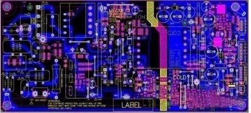
7. Evaluation of PCB Examples
Based on key PCB layout points discussed earlier, you can check if board is well made. I think this is a good place. Of course, there will always be defects, and you can let them down as well. The single-sided board is so compact that it can be made. It is not easy to reach this place, you can use this board for teaching and discussion! Later I will explain and learn about this board, let's enjoy it first.
VIII. Understanding four main circuits in PCB design (The main requirement for PCB layout is that four main circuits have a small area)
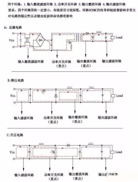
Besides, absorption loop (RCD absorption, MOS tube RC absorption, and rectifier RC tube absorption) is also very important, and it is also loop that generates high frequency radiation. If you have any questions about above image, please discuss it. Do not be afraid. Any question, as long as it is a question about a problem, discuss and study together to make more progress!
9. Hot spot (floating point) and ground wire of PCB design:
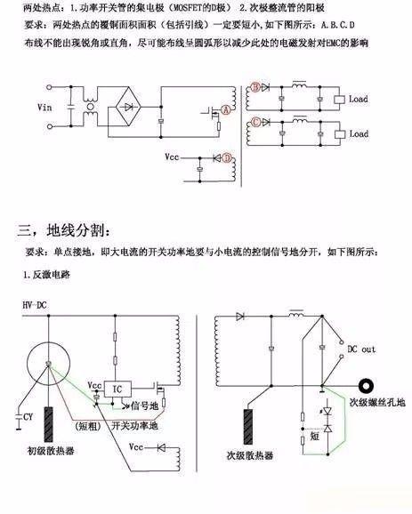
Note.
1. Particular attention should be paid to hot spots (high frequency switching points), which are high frequency emission points, and location and routing have a great influence on EMC.
2. The loop formed by hot spots is small, wiring is short, and thicker wiring, better, but there is enough current.
3. The ground wire must be grounded at one point. The main power ground is separate from signal ground, and sample ground is separate.
4. The radiator ground must be connected to main ground.
10. EMC elimination experience
This is all personal understanding and may differ from traditional textbooks. Please think for yourself. In any case, I think that many general textbooks are not used on my own resume, so I'm showing off. There are a lot of things that I want to say that can be a bit confusing, but it's all practice.
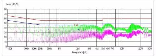
How to understand EMS generation and results measured during test: in simple terms, how to prescribe right medicine in many cases, how to compare and analyze results with power supply after receiving first round of test results; main idea is this:
1. For conductivity, test range standard is 15K-30M, and general EN55022 standard starts at 150K. How did transmission source come about? For low frequency, it is mainly switching frequency and its multiplier (shown below), which cannot be solved from source, and switching frequency cannot be eliminated. Of course, you can change switching frequency, which only shifts test results, and is not completely eliminated . This can only be solved with a filter. Generally speaking, use of high flux materials such as R10K for low frequencies has a good effect. The size of magnetic ring is related to your power. Generally, its inductance can reach 10MH, or even more, than 20MH. Capacitors can generally be dealt with very well, and low frequency is not difficult, real difficulty lies in high frequency. I personally think reason for high frequency is much more difficult. This is caused by switches, transformers, and inductance, then there is everything is in a state of switching, it can exist anywhere (how to judge a specific place, following explanation), some research is required here, source detection can not necessarily solve source, there may be an improvement, or cooperate with filter. For high frequencies, use a low flux material such as a nickel-zinc ring, inductance is usually UH level, with a suitable Y capacitor (for more complex power supplies, it is recommended to leave a few more positions of Y capacitor when placing board for easier correction). 2. Some methods of coordination, many textbooks mention increase in cocapacitor X to evaluate differential or common mode, which is of some value, but may not help much in reality. Capacitor X in design. And increasing X capacitor can solve differential mode problem, which is also nonsense, which is why many tutorials give specific guidance that I personally find useless. I think there are some better methods: one is to compare ground and obscure ground to summarize differences. Without ground, it can be worse because structure of system has fewer conduction paths, it can also be improved by indicating that it is being transmitted to port through ground loop. The specific solution is to adjust capacitance of circuit ground Y point and add magnetic balls. Second, place magnetic ring on input port. If low U ring improves, adjust first stage filter inductance. 3 Sophisticated systems pay attention to EMI shielding measures. If measures fail, check design of printed circuit board, which will be indicated in design of printed circuit board. 3. For radiation: you need to find a source to solve this problem. Pay attention to first test result. If it exceeds 30M, it is due to grounding. Locate ground in system and evaluate if ground is good during test. Sometimes input lines are affected. 2. Within 40-100m, this is usually caused by MOS tube turning on and off. Sometimes it is directly judged whether it is turned on or off due to local inconvenience, and observation results can be adjusted to check (of course, this will cost money, and I I'll explain how to use it later) Oscilloscope to judge, it's a secret trick). 3 Most of above 100m is caused by diodes. Correct absorption capacitance of diodes. Some of high-power diodes can be synchronous rectification. Change absorption loop of MOS tube. Remember that sometimes when adjusting C, you must cooperate with R to correct. There are too many things to say, let's add concrete examples later, I played so much at first, anyway, I worked hard enough, it's hard to resonate, after all, everyone's rectification experience is a lot different, so just give it to me Let's inspire newbies and friends and I'll give examples later.
Eleven, location and routing of filter capacitor
The filter capacitor wiring plays an important role in filtering effect. If wiring is incorrect, it may lose its proper filtering effect.
Figure 1 is a rectification and filtering method on secondary side, so that effect of two capacitors can be separated to avoid failure of second capacitor in rectification circuit.
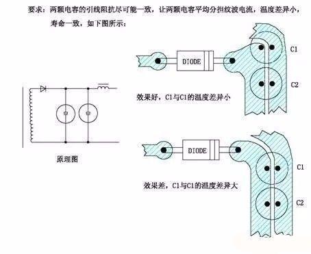
Figure 2: Output filter capacitor wiring should not be connected (i.e. shunted). If wiring is poor, output ripple will be very low.
12. Scheme and EMC of LLC circuit
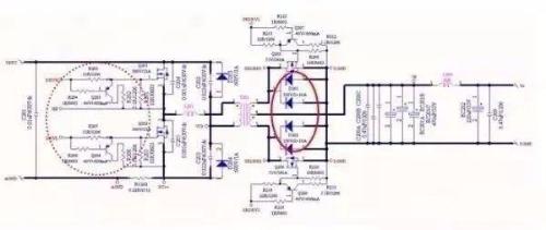
The LLC scheme is most familiar to everyone. The dotted circle is drive circuit, which, when designing circuit, is placed close to MOS tube, that is, drive provided by IC only needs to run two wires. to drive chain. close to avoid interference (at same time, pay attention to driver interference for sensitive signals when wiring, which is both a sensitive signal and a source of interference); once driver is disturbed by power supply, it is conceivable. Similarly, MOS rectifier tube synchronous drive should be close to rectifier synchronous tube. When designing a circuit diagram, it can be easily understood by placing it as shown in figure. If you give this circuit to a PCB engineer to lay out board, it will. It's very intuitive how to lay out wiring. If you draw a mess, many circuit board engineers can easily place wrong board if they understand circuit well. In addition, there is an important loop on primary side, and loop area formed by PFC capacitor, MOS tube, transformer, resonant inductor, and resonant capacitor is small. The rectification and filtering loop on secondary side is also important, and capacitor wiring is also very important, as mentioned earlier. Pay attention to distance between high and low voltage when connecting. In some places, voltage floats and must be considered as high voltage, for example, top drive of tube and corresponding reference voltage. Regarding EMC, LLC turn-on is a software switch that has little to no effect on EMC, focusing on effect of turn-off speed on EMC and MOSFET capacitance. Tube junction capacitance has a big impact on EMC. Incorrect selection of capacitors or no capacitors (MOS tube itself also has junction capacitance) can affect EMC, which is a key point to pay attention to; capacitor in this figure, and it can also be very effective to place Y capacitor on positive or negative side of MOS tube. It is good to filter out switch noise; If you have any doubts about this scheme, you can discuss it and grow with each other in discussion!
Thirteen, PFC circuit design and layout
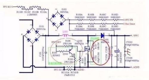
The figure above shows a typical BOOST PFC circuit:
The green box on left is drive layout, same as previous LLC topology drive, next to MOS, and is shown in circuit diagram. Part of green dotted line on right represents peak absorption circuit when MOS tube is turned off, and loop formed by MOS tube should be smallest; two other important circuits are MOS tube loop open (red dotted diagram), other is MOS tube off loop (solid red line); loop area should be as small as possible;
Fourteen, magical use of magnetic rings in EMCSome products are difficult to deal with EMC at source, and magnetic ring filtering can be used, of course. The magnetic ring I'm talking about here has two meanings. On one hand, it is a filter inductor at input and output. By using magnetic rings of different materials, different coils will have corresponding effects. On other hand, this means direct coverage of input and output lines. The magnetic ring can sometimes play a magical role, but not in all cases, at least it can be used as a basis for judgment.
The blue and black lines in image above represent positive and negative terminals of output, and a magnetic ring is installed on them, which eliminates high frequency end caused by output rectifier; sometimes port interference may be ineffective if a filter is added to PCB. Installing a magnetic ring on output line has an unexpected effect.
Fifteen, PCB layout key signal
Note.
1.CS signal (sampling signal): pull it out of sampling resistors R25 and R26. Note that ground wire of IC is based on sampling resistor, and positive and negative differential wire of sampling resistor pulls to CS pin of chip and to GND pin microcircuits.
2. The excitation signal pulls IC drive pin out of drive circuit, and be careful not to interfere with CS pin; as shown in figure, three wires are laid side by side, and ground wire is placed between driver and CS line to reproduce a certain shielding effect;
3.For double-sided boards, it is best to shield IC on ground layer. The ground network should be drawn from IC ground. The non-critical GND signal can be drilled directly. The key signal ground needs to be grounded at one point and directly connected to IC;
4. FB feedback network signal, pay attention to routing and single point connection to IC;
5. The RCD absorption network should not be placed in main circuit;
6. The VCC rectification and filtering ground must be connected to main power supply ground, and secondary filter can be connected to IC ground;
7. The capacitor Y wiring is connected separately and must not be confused with main power to avoid interference.
Sixteen, power and control main circuit diagram
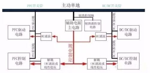
Many people may see this image, but it has its head in clouds, so here's a general introduction:
1. The KKM driver and IC are connected to KKM tube, or rather to ground of selective resistor;
2. The drive ground and control ground of DC-DC part are connected to sampling ground of DC switch tube part;
3. The control ground of auxiliary supply part is connected to auxiliary source MOS tube sampling stage, and MOS tube ground is then connected to main power supply ground;
4. The power supply ground of each IC is connected to IC ground through auxiliary power supply EC filter. Note that RC filter is located close to IC.
Summary: Pay attention to single-point grounding of each, and ground line is not tangled, which is one of most important places for wiring! Seventeen, analysis of electromagnetic field shielding mechanism Figure 1: Magnetic field shielding principle
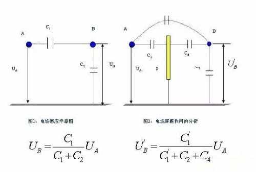
As shown in figure: The interference of input and output electric field can be coupled through capacitive transmission. If a shield plate is added, size of C4 will be increased and C1 will also be reduced, which will weaken electric field. field interference;
Figure 2. Magnetic field shielding principle
As shown in figure, magnetic field shielding characteristics are different from magnetic field characteristics. Shell shielding is required, and electric field only needs a flat shielding plate, so heatsink shielding provides electric field shielding, and some use closed power supply shell to play a role of magnetic field shielding;
Magnetic field shielding principle: The magnetic field passing through protective cover changes magnetic circuit, causing magnetic field lines to propagate, and intermediate magnetic field interference achieves purpose of shielding.
Eighteen, switching devices and EMCUnderstanding devices is also of great importance for EMC, such as MOS lamps, MOS main switch is one of important sources of EMC, and switching on and turning off rectifier will also produce high-frequency radiation (the principle is that current generates a magnetic field, and changing current generates an electric field); of course, main introduction of semiconductor switching devices and other inductive transformers will not be explained here. Which parameters of switching devices have an important influence on EMC, we often talk about fast lamps, what is benchmark for slow lamps? We all know that fast lamps have low turn-on loss and we like to use them for high efficiency, but in order to smoothly pass EMC, we must forego efficiency and reduce switching speed to reduce switching radiation. For MOS lamps, turn-on speed is determined by drive resistance and capacitance of input junction, and turn-off speed is determined by output junction capacitance and internal resistance of lamp.
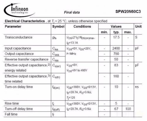
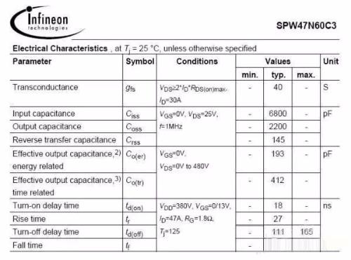
See The two pictures above are different types of MOS lamps. Compare capacitance of input and output junctions, 2400 and 800 pF, 780 pF and 2200 pF; this time switching speed should match excitation resistance. ; generally, drive resistance is more than 10-150 ohms, and choice of drive resistance is related to junction capacitance. The drive resistance of fast board can be increased accordingly, and drive resistance of slow tube can be reduced accordingly. For diodes, there are Schottky diodes, fast recovery diodes, conventional diodes, and SIC diode, which is used less frequently. The switching rate of SIC diodes is almost zero, which means there is no reverse recovery and no switching radiation. and losses are also smallest, only minus is high cost, therefore it is rarely used; second is Schottky diode having low forward voltage and low reverse recovery time followed by fast recovery and conventional diodes, it must be in losses and EMC There is a trade-off between them, generally measures such as changing EMC can be taken to eliminate absorption and installation of magnetic balls.
Nineteen, EMC filter
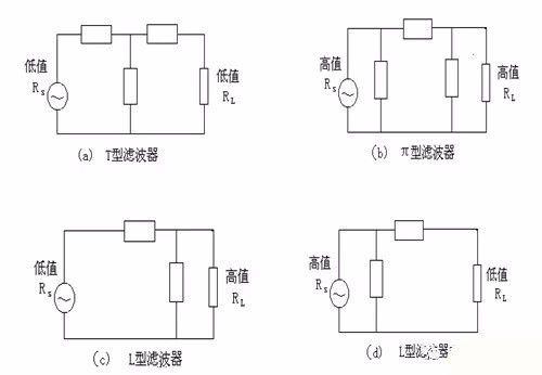
The choice of filter architecture is very important for a filter. In different cases, filter is based on impedance matching to achieve filtering effect. You can refer to how to filter according to principle of this figure, such as most commonly used output rectifier bridge After that, a π-type filter is used, and output uses an LC filter.
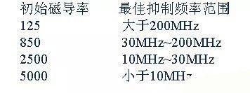
The filter material is also very important to design of filter inductor. Materials with different initial permeability will work in different frequency ranges. If wrong material is selected, desired effect will be completely lost.
20. High-frequency equivalent EMC feedback model analysis
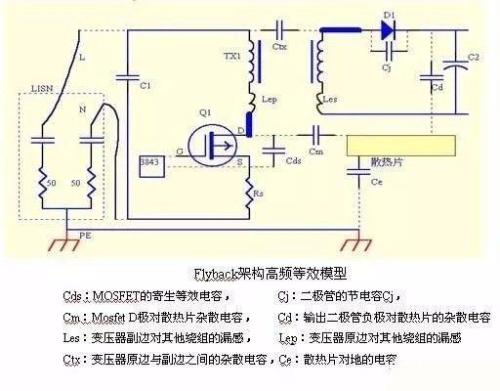
First understand EMC from simplest model: EMC path, of course, cosmic radiation is connected with loop, and loop is also formed by path; analyze flyback high frequency equivalent model to help understand EMC formation mechanism; our test receiving equipment will receive conduction from L, N terminals, in order to reduce received interference, we must allow interference to pass through ground loop, and not flow from L, N ports to receiving equipment; at this time, our EMI inductance and Y capacitance can be realized by impedance matching; in addition, interference of primary side can be connected to secondary side through primary and secondary capacitance Y, parasitic capacitance of transformer and ground, so as to form more loops; of course, some junction capacitance parameters such as MOS tube junction capacitance and radiator junction capacitance can also shape flow path;
21. Radiation shape and frequency distribution
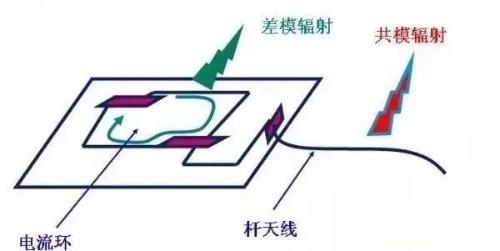
This picture might be a bit abstract, but it's hard to be specific about EMC. We need to give us some clarification. It can be seen that differential radiation exists as a loop, while common-mode radiation is emitted as an antenna; therefore, this just confirms previous statement that when we lay out circuit breaker stub diagram and do not take sharp corners when wiring, usual wiring is 45 degrees, and it is best to use circular arc routing. Of course, routing efficiency will be relatively low.
The basic knowledge of these principles is well understood, which is very useful for actually doing job and EMC layout. If there is no such understanding, it may be useless as it cannot provide a direct method and must be combined with other knowledge. Moreover, many of the principles and things mentioned here are not seen in many EMC materials, and they are not so concentrated that they need to be experienced repeatedly!
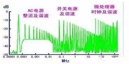
As shown in figure, relationship between some frequency terminals and generating parts of switching power supply is just a general rule, so don't believe it completely, why can't you completely believe it? The law does not work in all situations, and difference between different power supplies is also great, so principle is to help you analyze, not rigidly follow method;
Twenty-two, EMC example
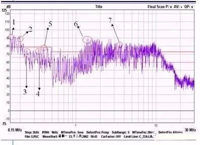
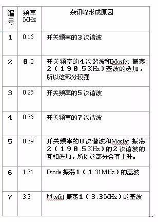
According to conductance example, key to frequency distribution point is relationship between specific data and fundamental frequency. of course, how these frequencies pass through filter Ways to solve this were mentioned earlier. Let's add some mystery to EMC, how it came about, it's not a mystery anymore, and it's not just stupid use of filters to solve a problem!
—— End—
Related
- Diagram of relationship between PCB layout and EMC
- PCB design guidelines: safety regulations, layout and wiring, EMC, thermal design, process engineering.
- Do you know layout requirements of some special devices in PCB design?
- Should PCB trace angle be 90°? — Jumping guide to PCB layout pit
- Daniel's Summary: The details and experience of 30 PCB layouts are wonderful.
- Senior EMC Engineer Resume: EMC Troubleshooting Process and Common Problems
- Suggested collection: Capacitor filtering analysis and EMC suggestions.
- Summary of Common PCB Repair Techniques
- How many types of pads have you seen in PCB design?
- Why can't crystal oscillator be placed on edge of the PCB?
Hot Posts
 How to distinguish induction from leakage, we will teach you three tricks! Ordinary people can also learn super practical
- What is drowning in gold? Why Shen Jin?
- This is a metaphor for EMI/EMS/EMC that can be understood at a glance.
- How many types of pads have you seen in PCB design?
- Summary of Common PCB Repair Techniques
- What is three anti-paint? How to use it correctly?
- Knowing these rules, you will not get confused looking at circuit diagram.
- How to make anti-interference PCB design?
- Can diodes do this?