Location:Home Page > Archive Archive
You must learn drawing techniques and skills of 18 special circuit board routes.
2023-04-22【Archive】
Question 1. AD fabric serpentine method
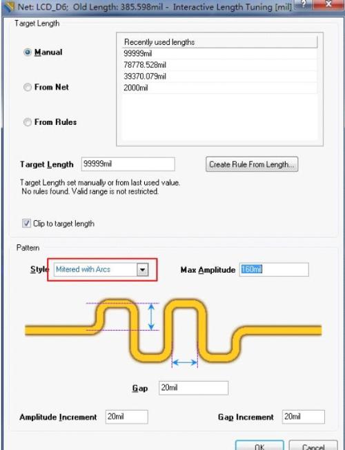
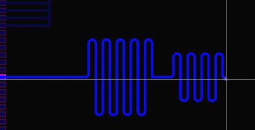
If you select Interactive Length Adjustment in Tool, you need to lay out wires first and then change them to a serpentine shape. Here you are using serpentine directly when wiring: first P->T routing and then Shift + A to switch to serpentine routing.
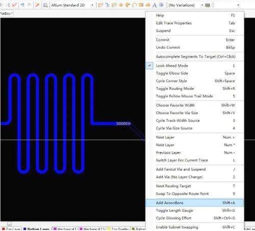
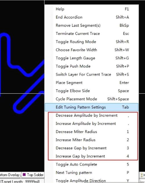
Press Tab to set attribute, select arc type, Max Amplitude to set maximum amplitude, Gap is interval (I don't know if this translation is correct), bottom left is amplitude increment. , and on right - interval increment.
Then start wiring.
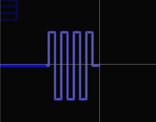
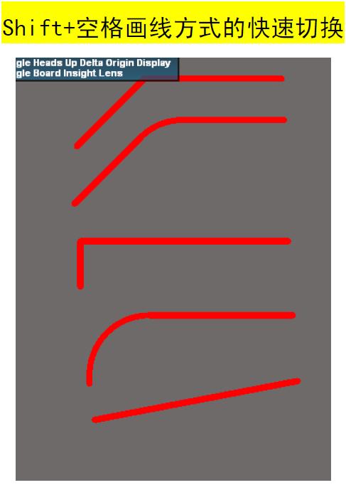
Make edge 'round' - press shortcut key '2', this will increase radius of arc, and when it is increased to maximum, two 1/4 arcs will connect directly, forming a 180 degree semicircle. Shortcut key "," "." can adjust amplitude.
If you don't remember keyboard shortcut, don't worry, press "`" at any time to display currently supported operations.
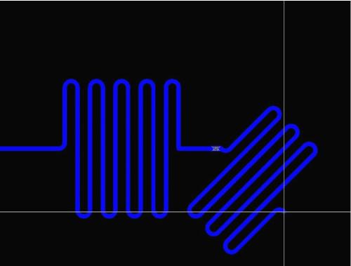
You can see length of network, there is more than one place.
Single length. The same length can be routed using adjusters.
Question 2: Remove layer of solder on high current track
There are two things to note here. Firstly, Paste layer is a true tin sprayed layer, but trace has a soldermask layer by default, so it's useless to use just Paste, so you need to use Solder. , this layer The drawn part is not solder resistant, so "paste + solder" method can be used to draw tin sputtering line. If there are traces on board, you can directly use corresponding layer's solder to open window.
Question 3: drawing of a bus
Altium Designer supports simultaneous routing of multiple nets, and routing can start from pads or from beginning of lines. Hold down Shift key to select multiple networks, or use mouse to select multiple networks, select menu command PLACE >> Interactive Multi-Routing, and click bus routing tool on routing toolbar to start routing bus. you can place, you can switch layers of straight lines, you can click commas and dots. The distance between branches is adjustable.
Meanwhile press 2 to add transitions, L to change layers~
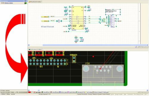
Question 4. From schematic to board
On circuit diagram, use mouse to select a circuit or multiple devices, press T->S, you can immediately switch to PCB and select these devices at same time.
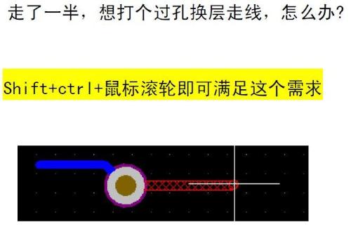
Question 5. Changing layers, working with vias, working with routing
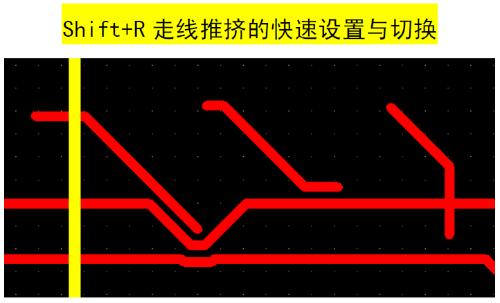
Question 6. Quick setup of wiring and connection method
Question 7. Inserting simple graphics on a printed circuit board
Inserting metafiles makes it easy to create mechanical layer design documents. Using same paste command (Ctrl+V) as in Windows, any metafiles from clipboard can be pasted into PCB editor. Metafiles can be lines, arcs, simple fills and True Type text, any imported data will be placed on current layer.
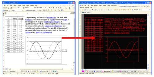
Copy data from Word or Excel to board. Supported metafiles include bitmaps, lines, arcs, simple fills, and True Type text, making it easy to insert logos and other graphics.
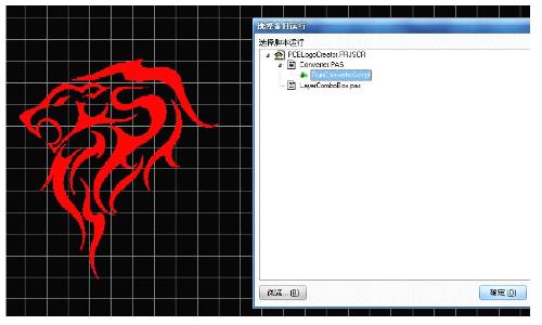
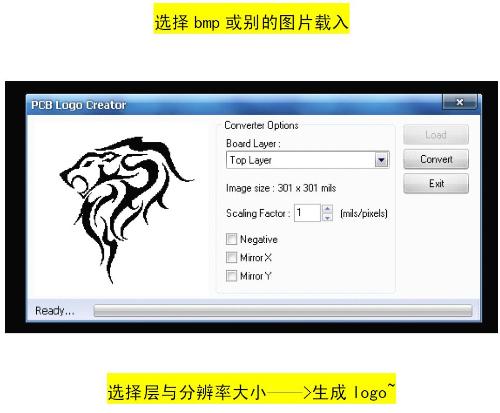
Question 8 Manufacturing boards of complex graphic elements (logo)
Question 9. Mesh setup and capture
Visual and electrical meshes in Altium Designer can be set in multiples of captured mesh (Design>>Board Options).
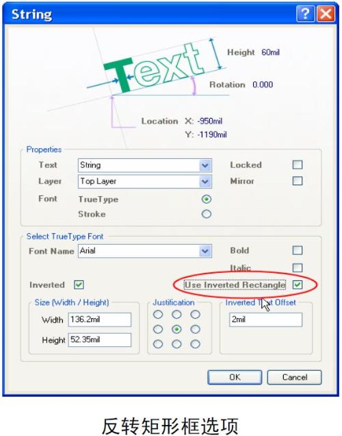
Question 10: Reverse text silkscreen color output and position adjustment
A new valid string property window option has been added to PCB Editor. The new option can define a different rectangular border range for inverted text using True Type fonts instead of using borders of inverted text itself as before.
Reverse size (width/height): sets width and height of inverted text rectangle
Setting layout: defining relative position of text in text field
Reverse text offset: define offset of reversed text relative to rectangle
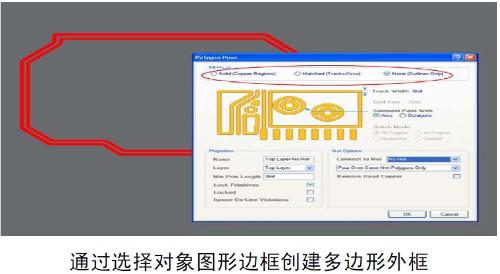
Question 11 Miscellaneous~filling polygons
Using "Select Objects to Define Polygon Shape" feature makes it easy to create company logos or polygons from external sources such as DXF, AutoCAD, etc. Polygon shape definition is divided into two steps: first, define a polygon area from menu Tools>>Polygon Fill>>Define from Selected Objects, then right-click on polygon fill area and select Properties option from menu. popup menu, now you can set it to fill dialog box mode.
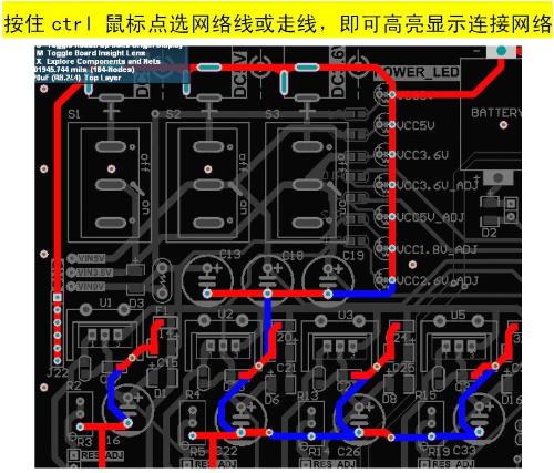
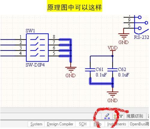
Question 12: Select a net on board
Question 13. Single-level operation and custom operation
For a messy device layout, this is already very troublesome. If you want to lay wires in chaos, it's not easy. You can use Shift+s in AD to solve this problem (in board edit state) :
Also, I learned of a setup method from Internet that was a little tricky at first, but after learning, it turns out to be very practical.
Method:
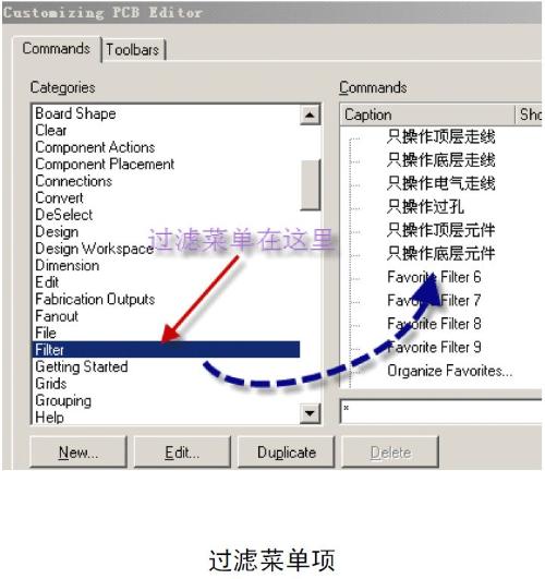
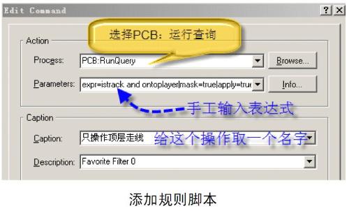
An expression that only works with top-level routing: expr=IsTrack and OnTopLayer|mask=True|apply=True
An expression that only works on bottom layer: expr=IsTrack and OnBottomLayer|mask=True|apply=True
Electrical wiring only expression: expr=IsTrack and IsElectrical|mask=True|apply=True
Expression for active vias only: expr=IsVia|mask=True|apply=True
An expression that only works with top-level components: expr=IsComponent and OnTopLayer|mask=True|apply=True
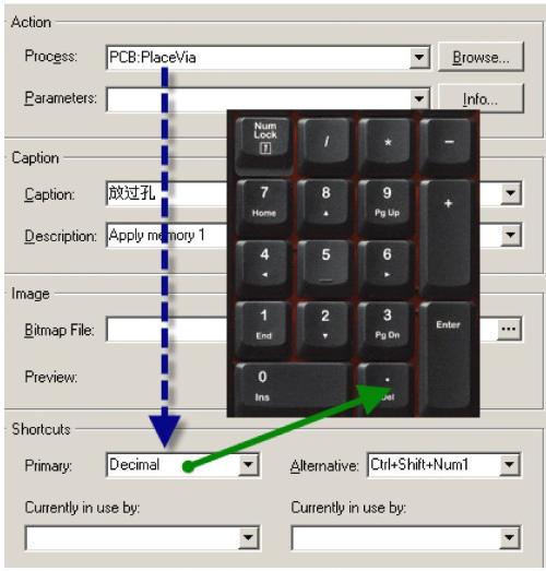
Set up multiple via sizes, use number keys in a small area of the keyboard as shortcut keys, 3 means through hole with 0.3 aperture, 4 means hotkey 5 with 0.4 aperture, so you want to use any size through hole can be easily adjusted. I know that AltiumDesigner itself can use "shift+v" keyboard shortcut to call up vias of various sizes that you filled in during routing, but I place vias myself. If you want to change size, you have to press Tab key and rewrite size data of vias, which is a lot of work. Instead, use following method:
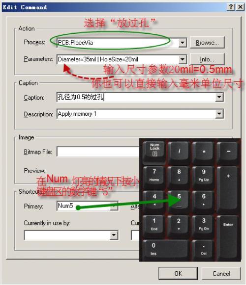
Altium originally used "P" + "V" for default via placement, but now I use "." in small keyboard area to perform same function:
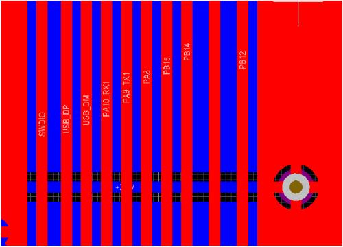
Question 14 Operation of multilayer lines
Some people ask how this line is drawn:
Answer: Draw them one by one.
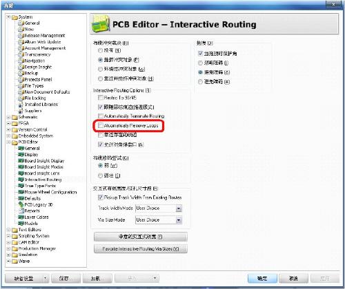
How do I set lines to overlap? Options, PCB Editor, Interactive Routing, Interactive Routing Options, Remove Contours Automatically can be deselected.
It's okay if you don't draw one at a time, Place is Region, just put a polygon area, but be careful, don't add network yourself. will turn green.
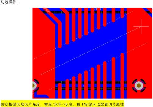
Question 15. Wire cutting operation
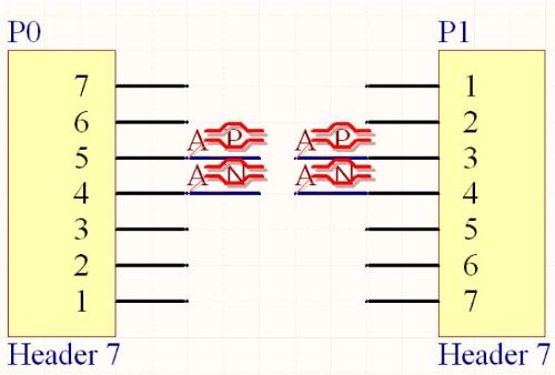
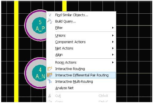
Question 16. Installing and laying equivalent differential lines
Many beginners will hear word "differential line". In fact, it is not difficult to talk about a differential line. It's just a connection method. This is much simpler than equal length line mentioned earlier, but there are certain rules for setting it up:
Place components and draw signals of differential pair. The difference pair naming conventions have same name, and suffixes are marked _P and _N respectively. Then select Place Differential Pair Directives and place differential pair symbol.
After upgrading to PCB
It's okay~
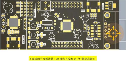
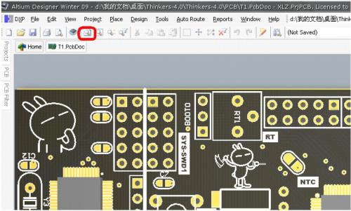
Question 17. Working with 3D display
Your main window can be displayed in both 2D and 3D. Switching between 2D and 3D can be done with shortcut key "3" to switch from one 2D view to previous 3D view; press "0" to smooth. Shift+right-click+drag to rotate the 3D view.
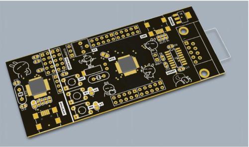
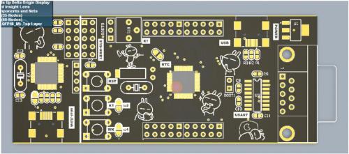
Haha~ Here's a board I recently designed~Small STM32F103C8 board with JLINK emulator~
Question 18. Fast zoom in and out
There are many ways to make a window bigger, but there are only 3 more practical ones. Below is an introduction:
1. Full interface
2, ctrl+wheel (center of mouse is center of zoom in and out)
3. Press and hold scroll wheel for a long time to turn it into a magnifying glass, and drag your mouse back and forth to quickly zoom in and out.
Related
- You must learn drawing techniques and skills of 18 special circuit board routes.
- Is printed circuit board covered with copper very “up to mark”? One article to help you get practical guidelines and norms
- How many of these free and easy to use circuit design programs have you used?
- List of 5 Most Practical Network Analysis Techniques! must watch
- Experience in recognition of circuit diagrams of electronic circuits and method of circuit analysis
- Several Effective Circuit Analysis Techniques
- Do you know layout requirements of some special devices in PCB design?
- Optocoupler and application circuit
- What is difference between surge device, lightning arrester, leakage protection, circuit breaker and circuit breaker? Come and get knowledge
- The best switching circuit design process for power supplies is a must for engineers!
Hot Posts
 How to distinguish induction from leakage, we will teach you three tricks! Ordinary people can also learn super practical
- What is drowning in gold? Why Shen Jin?
- This is a metaphor for EMI/EMS/EMC that can be understood at a glance.
- How many types of pads have you seen in PCB design?
- Summary of Common PCB Repair Techniques
- What is three anti-paint? How to use it correctly?
- Knowing these rules, you will not get confused looking at circuit diagram.
- How to make anti-interference PCB design?
- Can diodes do this?