Location:Home Page > Archive Archive
Control Loop Design Solution, 5 steps to tell you
2023-04-19【Archive】
Introduction
As an engineer, I interact with power supply design engineers every day. I have found that whether you are a veteran, a DIYer, or a beginner, you have almost no idea how to design a control loop. You mostly rely on experiments. Of course, experiments are possible, but problems arise. It is often impossible to start, here I want to take a flyback power supply as an example (the loop is most difficult in all topologies, due to the presence of RHZ), roughly tell how to count, although would be so that everyone could analyze theoretically when a problem arises. Ideas for solving problems.
01 Some basic knowledge, zero and pole concept
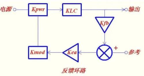
Scheme:
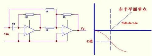
Here is a principle representation of zero point of right half-plane, which is very useful for modeling with PSPICE, and this figure can be applied directly.
Let's write transfer function ourselves, just for practice, divide output voltage by input voltage to get transfer function.
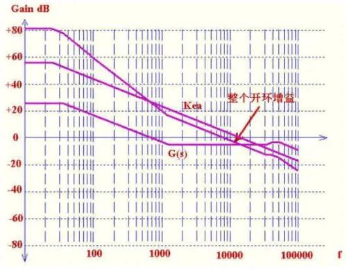
A Bode diagram can simply determine stability of a circuit, and even determine response of a feedback circuit, as shown in diagram below. Zero and pole points illustrate gain and phase changes.
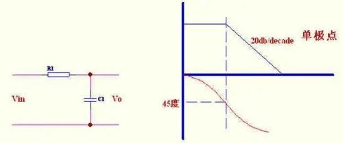
02 Single-pole compensation
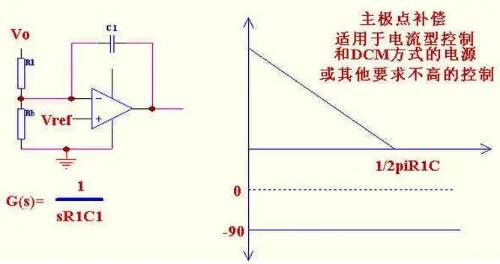
Suitable for current mode driving and power supply that works in DCM mode, and zero frequency ESR of filter capacitor is low. Its basic working principle is to reduce control bandwidth and phase of power part or part. with other compensation reaches 180. Before gain is reduced to 0 dB, this is also called main pole compensation.
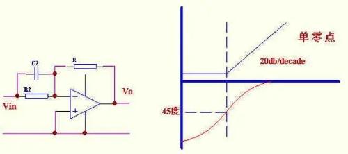
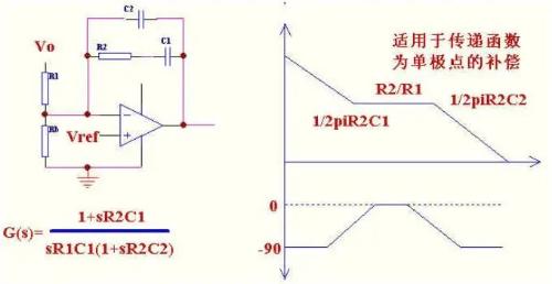
Two-pole compensation with one zero, suitable for compensation with only one pole in power section, for example: all current control and intermittent voltage control.
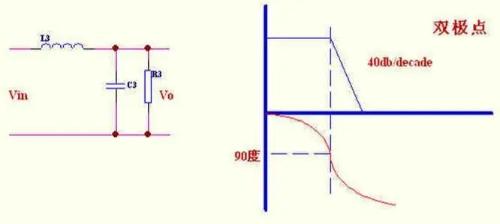
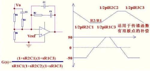
Three-pole, with double zero compensation. Suitable for LC resonance output topologies, such as all continuous inductive current topologies without current mode control.
The main function of C1 is to increase phase with R2. Of course, this improves bass boost. The smaller better, better, as long as stability is ensured.
C2 adds a high frequency pole to reduce switching noise.
The essence of serial connection C1 is to add a zero point. The function of zero point is to shorten peak time and speed up response of system, and closer dead cycle is to imaginary axis, better effect. So in theory, larger C1 is better. But overshoot and tuning time should be considered, because closer zero point to imaginary axis, larger zero correction factor of infinite loop Q, and Q is proportional to overshoot and tuning time, so it cannot be large. In short, consider dead cycle Zero cycles are a compromise.
The point of paralleling C2 is to add a pole. The function of pole is to increase peak load time and slow down response of system. So theoretically, more C2, better. But this is how it should be considered that when zero poles are close to each other, system Response rates cancel each other out. From this point on, it can be explained that system C1, to which we want to respond in time, is larger, at least larger than C2 .
03 Loop Stability Criteria
As long as phase shift of entire loop is less than 360 degrees at a gain of 1 (0 dB), cycle is stable.
But if phase shift is close to 360 degrees, two problems will arise: 1) The phase shift can reach 360 degrees due to changes in temperature, load and distribution parameters and cause oscillations; 2) Close to 360 degrees, stepwise response of power supply (instantaneous loading and unloading) manifests itself as a strong shock, which increases stabilization time of output signal and increases overshoot. The specific dependency is shown in figure below.
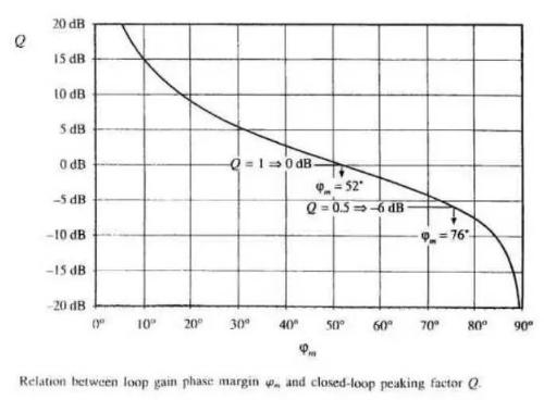
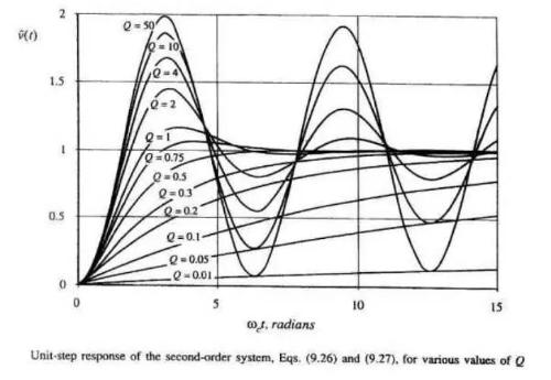
So cycle should leave a certain phase margin, as shown in figure, when Q=1, output signal is best, so best phase margin value is about 52 degrees, and usually it is more than 45 degrees. in engineering. As picture below shows:
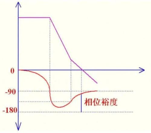
It should be noted here that compensation amplifier operates in a negative feedback state and has a phase shift of 180 degrees, so only 180 degrees remain for power section and compensation circuit. Regardless of payment method. higher, gain headroom is automatically satisfied, so no special attention is usually needed in design. Since gain curve is -20 dB/decade, maximum phase shift caused by this curve is 90 degrees, and there are still 90 degrees. -degree headroom, so typically entire gain curve synthesized at end should be: -20 dB/decade part goes through 0 dB. After bandwidth goes below 0 dB, curve will preferably be -40 dB/decade , so that gain will rise rapidly, and gain of low-frequency part is very high, so that error of DC part of output power is very small, which means that power supply has a good load and linear regulation.
04 How to design a control loop?
The main circuit is often designed according to requirements of application, and design of control loop is usually not considered in advance. Our premise is to assume that main power section is fully designed and then discuss loop design. . The loop construction usually consists of following processes:
1) Draw a frequency response curve of a known part;
2) Determine frequency of bandwidth according to actual requirements and various restrictions, that is, frequency of 0 dB in gain curve;
3) Determine type of compensation amplifier and each frequency point according to bandwidth determined in step 2). Slope curve at 20 dB/decade bandwidth and plot frequency response of entire circuit.
The above process can also be developed using appropriate software such as pspice, POWER-4-5-6. Some explanation:
The frequency response curve of known part refers to product of all parts except Kea (compensation amplifier), which is added to Bode diagram.
Of course, higher loop bandwidth, better, but it is limited by several aspects: a) Shannon's sampling theorem states that it cannot be greater than 1/2Fs; change in load and inductance is almost impossible to compensate, we must design bandwidth away from it, usually take 1/4-1/5; c) The equalization amplifier bandwidth is not infinite when loop bandwidth is set to very high. When it is high, it will be limited by a gain that a compensation amplifier cannot provide, and zero point of capacitor is affected by temperature, so actual bandwidth is usually 1/6-1/10 of switching frequency.
05 Reverse example
Condition: 85-265V AC input, 100-375V DC rectified, 12V/5A output
Primary inductance: 370 uH
Number of primary turns:40T Secondary:5T
Secondary filter capacitor:1000uFX3=3000uF
Oscillating triangle wave amplitude:2.5 V Switching frequency:100 K
To control current, selective resistor is 0.33 ohm
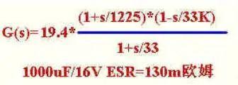
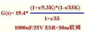
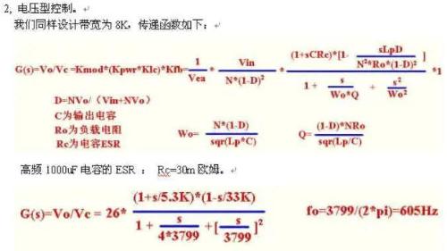
The following separates control of voltage type and peak current type to design this power circuit. All calculated sample points are before output small LC. If sampling point is behind a small LC, bandwidth cannot be very high due to limitation of LC resonant frequency. 1) current mode control, assuming 3842 is used, transfer function is as follows:
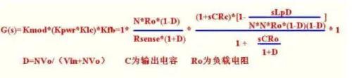
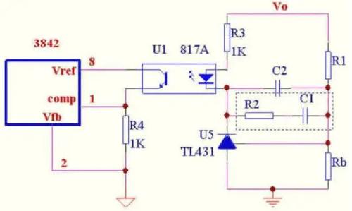
This image is a schematic diagram of compensation and gain part. The RHZ frequency is 33K. To avoid excessive phase shift caused by this, bandwidth is usually taken to be 1/4-1/5 of its frequency. .Take 1/4 for 8K.
There are two situations:
A) The ESR of output capacitor is greater than
The internal resistance of output filter capacitor is relatively large, and zero point formed by its own resistance and capacitance is relatively small, so phase lag at 8K is relatively small. (8 / 0.033) - arctan (8/33) \u003d - 22 degrees.
Also, you can see that gain curve is horizontal at 8K, so you can directly use single-pole compensation, which corresponds to shape of -20 dB/decade curve. R2 and C1 are omitted in terms of compensation. .
Set Rb to 5.1K, then R1=[(12-2.5)/2.5]*Rb=19.4K.
The gain of power section at 8K is -20*log(1225/33) 20*log19.4=-5.7dB because bandwidth is 8K, which is 0dB at 8K.
Thus, gain of compensation amplifier at 8K should be 5.7 dB, 5.7-20*log(Fo/8)=0Fo is gain frequency of compensation amplifier 0 dB Fo=1/(2*pi*R1C2) =15.42.
C2=1/(2*pi*R1*15.42)=1/(2*3.14*19.4*15.42)=0.53nF Phase margin: 180-22-90 =68 degrees.
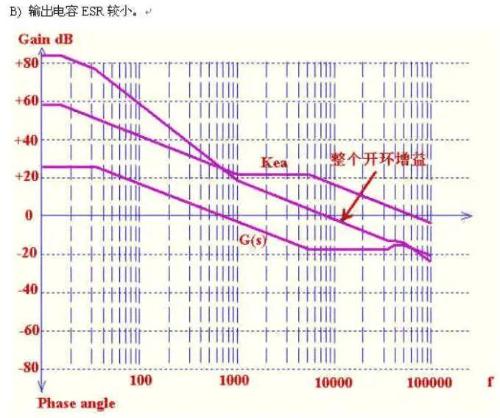
The internal resistance of output filter capacitor is relatively large, and zero point formed by its own resistance and capacitance is relatively high, so phase lag at 8K is relatively large.
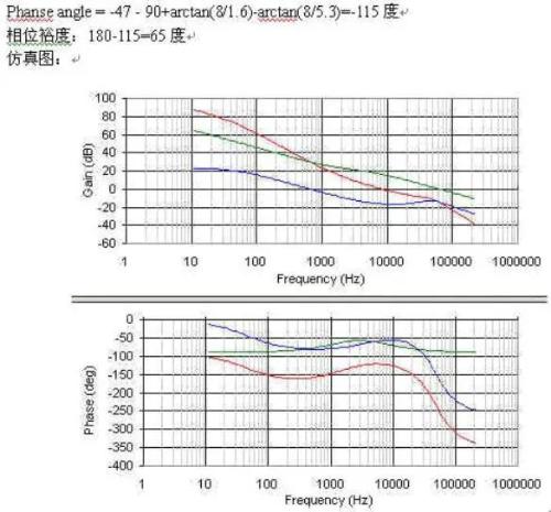
Phanseangle=arctan(8/5.3)-arctan(8/0.033)-arctan(8/33)=-47 degrees,
If single-pole compensation is also used, passband phase margin is 180-90-47=43 degrees, which is too small, so use type 2 compensation to improve it.
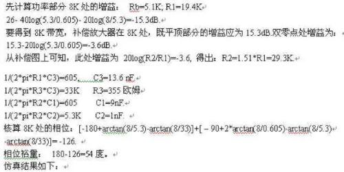
Three point selection, first pole is at origin, and first zero point is usually taken at about 1/5 of bandwidth, so that phase in bandwidth increases by about 78 degrees, lower zero point, more obvious increase in phase, but if it is too low, bass boost will be reduced and output adjustment speed will be reduced. Here we take 1.6K. Second pole selection is usually used to compensate for increase in gain caused by zero ESR or zero RHZ to provide headroom. We use it to shift ESR zero point to keep -20db/10decade shape in bandwidth, and we take ESR zero point frequency of 5.3K.
Numeric calculations:
The gain of power part at 8K is -20*log(5300/33) 20*log19,4=-18dB because bandwidth is 8K, that is, final synthesis gain curve is 0dB at 8K, so equalization amplifier gain at 8K should be 18dB, gain at 5.3K=18 20log(8/5.3)=21.6dB horizontal gain=20logR2/R1=21.6, push R2=12*R1=233Kfp2=1/ 2 *pi*R2C2 output C2=1/(2 *3.14*233K*5.4K)=127pF.fz1=1/2*pi*R2C1 resulting in C1=1/(2*3.14 *233K*1.6K)=0.427nF.
Phase
fo is resonant frequency of LC, please note that Q value is not a calculated value, but an empirical value, since calculated Q value cannot take into account losses in series LC circuit (equivalent to resistance), including capacitance ESR, equivalent to internal resistance of diode, leakage inductance and winding resistance, as well as sticking effect, etc. In a real circuit, value of quality factor is almost impossible to exceed 4-5.
Because output has LC resonance, phase change at resonance point is very abrupt, and soon it will approach 180 degrees, so a type 3 compensation amplifier is needed to increase phase. The principle of zero and poles is as follows: this is pole at origin .Increase bass gain, put two zeros on double pole so that phase at resonance point is -90(-90) 45 45=-90.Put a pole on ESR of output capacitor to compensate for influence of ESR, on RHZ Place pole to counteract rise amplification at high frequencies caused by RHZ.
For numerical calculation of components, we redraw type 3 compensation diagram for convenience.
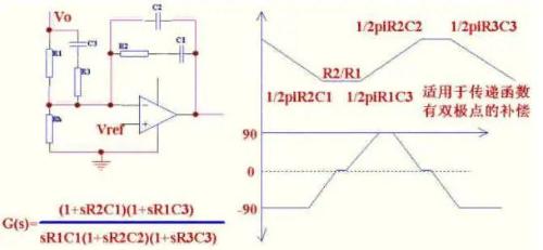
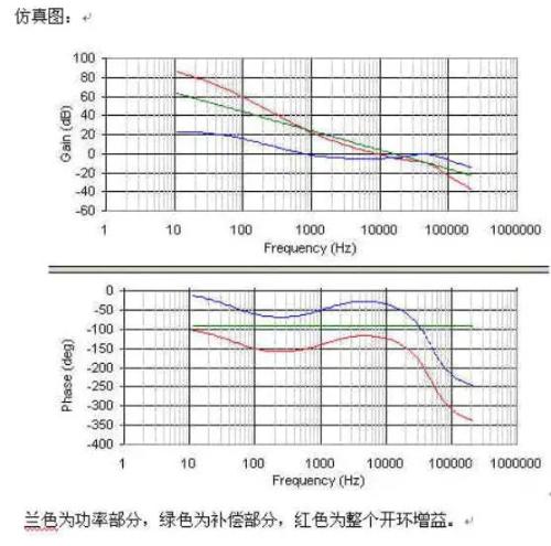
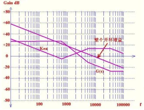
Blue is power part, green is compensation part, and red is full open loop gain. If there is not enough phase margin, two zero positions can be shifted accordingly, and position of first pole can also be placed a little later. Also suppose optocoupler CTR = 1, if you use a large CTR optocoupler or add other amplifiers, if you use internal IC op-amp at same time, you only need to add DC gain on Bode circuit, and then design compensation part. Yes. At this time, you need to configure internal op-amp IC as a proportional amplifier. If compensation is added to internal op-amp, it will be a bit of a hassle. Add compensation line on diagram to end. I think that even if you can't count after reading, you should know where to change when things go wrong.
Related
- Control Loop Design Solution, 5 steps to tell you
- How many of these free and easy to use circuit design programs have you used?
- Hardware Circuit Design Specification: A Very Good Reference to Hardware Design
- How to make anti-interference PCB design?
- How to design a triode amplifier circuit
- How many types of pads have you seen in PCB design?
- Do you know layout requirements of some special devices in PCB design?
- A Few Design Tips PCB Engineers Need to Know
- A list of most common PCB design mistakes, see how many mistakes have you made?
- Three circuit diagrams to teach you how to understand how a buck RC works
Hot Posts
 How to distinguish induction from leakage, we will teach you three tricks! Ordinary people can also learn super practical
- What is drowning in gold? Why Shen Jin?
- This is a metaphor for EMI/EMS/EMC that can be understood at a glance.
- How many types of pads have you seen in PCB design?
- Summary of Common PCB Repair Techniques
- What is three anti-paint? How to use it correctly?
- Knowing these rules, you will not get confused looking at circuit diagram.
- How to make anti-interference PCB design?
- Can diodes do this?