Location:Home Page > Archive Archive
Four Tricks to Make Your Boost Circuit Safer
2023-05-02【Archive】
The three most common block diagrams of switching power supplies are buck, boost, and buck-boost, none of which are isolated from each other.
The main character introduced today is a boost boost circuit, a boost converter (or called a boost converter), which is a conventional DC pulse boost circuit that can make output voltage higher than input voltage.
The following mainly describes basic principle, parameter design of boost circuit, and how to add a protection circuit to boost circuit.
1
Basic Analysis of Boost Schema
The boost circuit is a switching DC boost circuit that can boost output voltage over input voltage. This is a relatively common method for designing electronic circuits.
First, basic information you need to know:
Capacity prevents voltage change, passes high frequencies, blocks low frequencies, passes alternating current, blocks direct current;
Inductance prevents current change, passes low frequency, blocks high frequency, passes direct current, blocks alternating current;
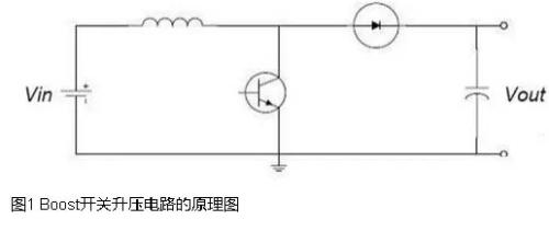
Assume that switch (transistor or MOS lamp) has been turned off for a long time, all components are in perfect condition, and voltage across capacitor is equal to input voltage.
The circuit will be described in two parts: charging and discharging.
1. Charging process
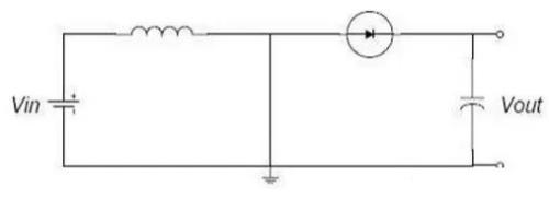
During charging, switch is closed (triode on), equivalent circuit is shown in figure above, and switch (transistor) is replaced by a wire. At this time, input voltage flows through inductor. The diode prevents capacitor from discharging to ground. Since DC is applied to input, current in inductor increases linearly at a certain rate, which depends on size of inductor. As inductor current increases, some energy is stored in inductor.
2. Upload process
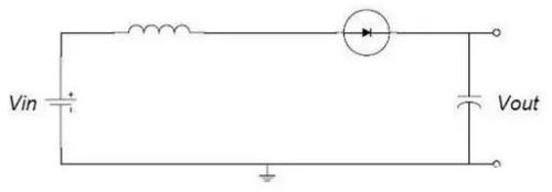
As shown in figure above, this is equivalent circuit when key is off (the transistor is off). When switch is turned off (transistor off), due to current holding characteristics of inductor, current flowing through inductor will not immediately become 0, but will slowly change from value at end of charging to 0. The original circuit was turned off, so inductor can only be discharged through a new circuit, that is, inductor begins to charge capacitor, and voltage across capacitor rises, and voltage is already higher than input voltage. The upgrade is complete.
Speaking of which, process of boosting is process of transferring energy of an inductor. When charging, inductor absorbs energy, and when discharging, inductor gives off energy. If capacitance is large enough, then a continuous current can be maintained at output during discharge. If this on-off process is repeated continuously, a voltage greater than input voltage can be obtained across capacitor.
2
Designing Boost Circuit Parameters
For Boost circuits, continuous mode inductor current is very different from intermittent mode inductor current. The output voltage of intermittent mode depends on input voltage, inductance, load resistance, duty cycle, and switching frequency. In continuous mode, output voltage depends only on input voltage and duty cycle.
1. Output filter capacitor selection
In a switching power supply, function of output capacitor is to store energy and maintain a constant voltage.
The choice of capacitor for boost circuit is mainly for controlling output ripple in specified range.
For a Boost circuit, capacitor impedance and output current determine size of output voltage ripple.
The impedance of a capacitor consists of three parts: equivalent series inductance (ESL), equivalent series resistance (ESR), and capacitance value (C).
In choke continuous current mode, size of capacitor depends on output current, switching frequency, and desired output ripple. When MOSFET is on, output filter capacitor provides all of load current.
2. Inductance
In a switching power supply, role of inductor is to store energy.
The function of an inductor is to maintain a constant current, or limit change in current in an inductor.
In a forced circuit, choosing an appropriate inductance is usually used to limit ripple current flowing through it.
The ripple current of an inductor is proportional to input voltage and turn-on time of MOSFET, and inversely proportional to inductance. The amount of inductance determines operating point of continuous mode and intermittent mode.
In addition to inductance of inductor, when choosing a coilInductance should also consider its maximum continuous or peak current, as well as maximum operating frequency.
The inductor current exceeds rated current or operating frequency exceeds maximum operating frequency, causing inductor to saturate and overheat.
3. MOSFET
For low power DC/DC converters, Power MOSFET is most commonly used power switch. The MOSFET cost is relatively low and operating frequency is relatively high.
When choosing a MOSFET in design, its conduction losses and switching losses are mainly taken into account.
The MOSFET should have a sufficiently low on-resistance RDS(ON) and a relatively low gate charge Qg.
3
Put protective clothing on your Boost chain
In previous part, we learned about Boost circuit and calculation of parameters of Boost circuit in terms of charging and discharging.
As a non-isolated boost circuit, Boost circuit has a simple structure, simple construction, and low cost. It is widely used in various boost applications that do not require isolation, especially in active PFC circuits.
Compared to BUCK or other isolating circuits, protecting a BOOST circuit seems more complicated.
For general protection circuits, when there is undervoltage, overvoltage, output overcurrent, short circuit, overvoltage or overheating at input, we will require circuit to automatically turn off output or implement hiccup protection so that this is useful for later load or circuit must be protected in time to avoid damage; but for BOOST circuit, due to boost inductance, output rectifier diode is in series in circuit between input and output, even if MOSFET drive is completely turned off, there will be no output. The voltage is lower than input voltage of inductor DC voltage drop and forward conduction voltage drop of diode, which means that output cannot be completely turned off, and protection effect we want is not achieved.
The following are a few solutions that can be used to protect BOOST circuits.

① MOS can be added to input for trip protection. This is a very good method, but driving MOSFET is more complex and requires a high voltage, high current MOSFET, which will increase system cost and reduce reliability. As a result, voltage at input terminal is relatively low, and it is more convenient to realize soft start when it is added to input terminal, reducing effect on MOS. However, due to lower output current, power consumption of MOSFET added to output is less.
② For similar products, Japan requires that output terminal be equipped with a protective device, usually a self-resetting fuse. In simple terms, resettable fuse is a PTC, which is not suitable for high power applications and will generate high losses. Adding a fuse to output terminal has relatively lower losses than adding a fuse to input terminal, and this method is cheaper and more economical.
③ It can be used to connect relays in series on busbar. When MOS is turned off, relays are turned off synchronously, so that main circuit can be turned off to cut off current circuit and further protect diode. The relay is a common protection method, but it also has disadvantages of having a short lifespan and easy ignition when switch is activated.
④ If you don't consider cost and complexity, you can create perfect protection scheme! But in fact, a short circuit at output is an example, and this "accident" is not worth spending much money on.
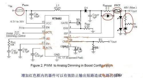
1. A fuse on Vin side must be installed to prevent a safety hazard due to MOS failure.
2. When output is short-circuited, fragile parts exposed to high current must be strengthened (Rsense in figure).
3. The BOOST output current is usually much less than input current, and even less than high current during a short circuit, so it is advisable to use a PPTC (self-healing fuse). The operating current of PPTC can be 2-3 times output current, and loss of PPTC under normal conditions is very small.
4. The EN voltage of Boost turn-on pin is taken from output. As soon as a short circuit occurs, EN=0V (voltage drops across PPTC), chip immediately stops working, and output voltage drops to approximately equal to input voltage, which can reduce short circuit protection. At same time, voltage on PPTC is reduced to reduce power consumption of PPTC.
5. When output short circuit is cleared due to presence of PPTC, EN will turn on again, IC will start and BOOST will work again.
No one pays attention to this area at present. Even for PFC circuits presented by large manufacturers, consequences of a short circuit in back stage can be imagined. The safest way to protect is to disable input. Current switching devices include transistors, MOSFETs, IGBTs, relays, contactors, etc. Different switching devices have different advantages and disadvantages.
Related
- Four Tricks to Make Your Boost Circuit Safer
- MOS tube drive circuit, how to make MOS tube turn on and off quickly?
- Principal analysis of BUCK / BOOST circuit, a summary is also in place
- How to design a triode amplifier circuit
- Three circuit diagrams to teach you how to understand how a buck RC works
- What skills should I pay attention to when designing a triode amplifier circuit? (Easy to understand)
- How to independently check malfunction of parallel resistance circuit? Chart details
- Hardware Circuit Design Specification: A Very Good Reference to Hardware Design
- step-down capacitor pay attention to these six points, do not need to worry about circuit analysis
- How to make anti-interference PCB design?
Hot Posts
 How to distinguish induction from leakage, we will teach you three tricks! Ordinary people can also learn super practical
- What is drowning in gold? Why Shen Jin?
- This is a metaphor for EMI/EMS/EMC that can be understood at a glance.
- How many types of pads have you seen in PCB design?
- Summary of Common PCB Repair Techniques
- What is three anti-paint? How to use it correctly?
- Knowing these rules, you will not get confused looking at circuit diagram.
- How to make anti-interference PCB design?
- Can diodes do this?